USB Connections and components
Overview
There are 2 downstream USB modules designed to receive and transmit serial data at full speed. One module is made up of a USB transceiver(mfg part# TUSB1106) and a Power-Distribution switch (mfg part# TPS 2552). The second USB block only had the transceiver (mfg part# TUSB1106.)
The TUSB1106 was chosen over other USB transceivers because of it's availability on DigiKey, it's unambiguous implementation for this specific project (it didn't require additional setting for differential mode data transfer) and it's well detailed datasheet.
The choice for the TPS2552 was a recommendation from Andrew. Moreover, i found the datasheet very detailed and fairly easy * to understand. *
Universal Universal Serial Bus Transceiver
- Manufacturer part#: TUSB1106PWR
- Digi-key part#: 296-21923-2-ND
- Package: 16-TSSOP
- Protocol: USB2.0
- Voltage Supply: 1.65V-3.6V
- Unit Price: $8.93
Pin Description
The Pin description below were extracted from the datasheet.
VCCIO
Supply voltage for digital input/ouput pins (1.65 to 3.6V). This pin must never exceed Vreg voltage
VREG
Internal regulator option. Regulated supply-voltage output (3 V to 3.6 V) during 5-V operation. A decoupling capacitor of at least 0.1 mF is required for the regulator bypass option. Used as a supply-voltage input for 3.3 V ± 10% operation.
VCC
Supply-voltage input (4 V to 5.5 V). Connect to Vreg(3.3). Can be connected directly to USB supply VBUS regulator bypass option.
VPU
Pullup supply voltage (3.3 V ± 10%). Connect an external 1.5-kΩ resistor on D+ (full speed) or D– (low speed). Pin function is controlled by input SOFTCON. SOFTCON = LOW – Vpu(3.3) floating (high impedance), ensures zero pullupcurrent SOFTCON = HIGH – Vpu(3.3) = 3.3 V, internally connected to Vreg(3.3)
D+
Positive USB data bus connection
D-
Negative USB data bus connection
/OE
Output enable (CMOS level with respect to VCC(I/O), active LOW). Enables the transceiver to transmit data on the USB bus input pad.
SPEED
Speed selection pin. Adjusts slew rate of differential outputs D+ and D- according to the transmission speed. For full speed (12Mbits/sec)
SOFTCON
Software controlled USB connection. Software-controlled USB connection. A HIGH level applies 3.3 V to Vpu(3.3), which is connected to an external 1.5-kΩ pullup resistor. This allows USB connect/disconnect signaling to be controlled by software input pad. Push pull, CMOS
RCV
Differential data receiver (CMOS level with respect to VCC(I/O)). Driven LOW when input SUSPND is HIGH. The output state of RCV is preserved and stable during an SE0 (SINGLE ENDED 0) condition output pad.
VMO
Driver data (CMOS level with respect to VCC(I/O), Schmitt trigger). Refer to Driving Function Table (pin OE = L) on datasheet using differential input data interface for TUSB1105 (pin MODE = H) and TUSB1106 input pad. Push pull, CMOS.
VPO
Driver data (CMOS level with respect to VCC(I/O), Schmitt trigger). Refer to Driving Function Table (pin OE = L) on datasheet using differential input data interface for TUSB1105 (pin MODE = H) and TUSB1106 input pad. Push pull, CMOS.
VP
Single-ended D+ receiver (CMOS level with respect to V). For external detection of single-ended zero (SE0), error conditions, speed of connected device. Driven HIGH when no supply voltage is connected to VCC(5.0) and Vreg(3.3) output pad.
VM
Single-ended D- receiver (CMOS level with respect to V). For external detection of single-ended zero (SE0), error conditions, speed of connected device. Driven HIGH when no supply voltage is connected to VCC(5.0) and Vreg(3.3) output pad.
GND
Ground Supply
SUSPND
A HIGH level enables low-power state while the USB bus is inactive and drives output RCV to a low-level input pad. Push pull, CMOS.
Functional Description
Pins
In order to bypass the internal regulator inside U1005 and U1006 (TUSB1106), Vreg and Vcc are both connected to the 3.3V power supply and decoupled with a 100nF capacitor to ground. This turns off the voltage regulator, thus enabling power saving.
Vccio should be independently connected to the 3.3V source (TUSB1106 datasheet recommendation pp6)
Pin SOFTCON should be set high to pull Vpu to the 3.3V at the output of the internal regulator through resistor R1014 connected to D+ for full speed configuration.
This pin is connected to PSC1_0 which is a simple GPIO pin on the MPC5200, and should be enabled for usage in the GPS simple GPIO Enable Register (Ref Section 7.3.2.1.2 on MPC5200B Users Guide, Rev. 1)
Integrated Circuits
U1006
U1006 from Texas Instrument is a Universal Serial Bus Specification REV.2.0 compliant transceiver designed to allow an easy handling of universal serial bus data transfer by the MPC5200. It is designed to work in full speed mode (12 Mbit/s) with flexible I/O voltage range from 1.65V to 3.6V which allows us to use the 3.3V power internally supplied on the STKxxx. The TUSB1106 allows only differential input mode which is the data transfer mode of choice required for this project; so no additional configuration were needed as with other transceivers (TUSB1105). U1006 is connected to the multipurpose Rocketbus connector which is the main connector of the Generic Front End node designed by the 2009 Capstone that provides interfacing between Flight Computer and the IMU module(Inertial Measurement Unit), the Avionics Power System module, GPS module, and Recovery module.
U1005
U1005 which is the other TUSB1106 is used with a power distribution switch (TPS2552) provides a second full speed USB compatible with USB Specification Rev.2.0 to connect the Flight Computer to the 802.11a USB adapter on the Telemetry Module
Resistors
R1107-R1110
These resistors are used for downstream configuration of the USB and for proper operation of D-/D+ data-bus in differential transfer mode. Their values were chosen as recommended by the datasheet.
The TUSB1106 datasheet recommends 15kOhm for these resistors
R1016, R1017, R1019 and R1020
These resistors are driver impedance matching resistors. The cable impedance must match the impedance of the high-speed and full-speed drivers. USB uses differential output driver to drive USB data signal onto the USB,so the driver impedance is very important in assuring optimal transfer of data. The USB Spec Rev2.0 says that When the full-speed driver is not part of a high-speed capable transceiver, the impedance of each of the drivers (ZDRV) must be between 28 Ω and 44 Ω, i.e., within the gray area in Figure 7-4 (on the USB Spec Rev2.0.)
The TUSB1106 datasheet recommends to use 33 Ohms resistors which complies with the USB Spec Rev2.0
Capacitors
C1019 and C1035
Used as decoupling capacitors for electrical noise suppression between the power supply and pins Vreg and Vcc on both U1005 and U1006.
C1019, C1019, C1035, and C1036
These are used as decoupling capacitors for electrical noise suppression between the power supply and Vccio, Vreg and Vcc on both U1005 and U1006.
The value chosen for both is 100nF (.1uF) (recommended by TUSB1106 datasheet) which will handle the high frequencies noise signals.
Precision Adjustable Current-Limited Power-Distribution Switches
- Manufacturer part#:TPS2552
- Digi-key part#:TPS2552DBVR-ND
- Package: SOT-23-6
- Voltage Input:2.5 ~ 6.5 V
- Unit Price: $9.9800
Pin Description
IN
Input voltage; connect a 0.1 uF or greater ceramic capacitor from IN to GND as close to the IC as possible.
OUT
Power-switch output
ILIM
External resistor used to set current-limit threshold;
/FAULT
Active-low open-drain output, asserted during overcurrent, overtemperature, or reverse-voltage conditions
EN
Enable input, logic high turns on power switch
GRD
Ground connection; connect externally to PowerPad
PowerPAD™
Internally connected to GND; used to heat-sink the part to the circuit board traces. Connect PowerPAD to GND pin externally.
Functional Description
Pins
Integrated Circuits
U1004
The U1004 (TPS2552) is a precision adjustable current-limited power-distribution switch from TI with operating range between 2.5V and 6.5V(allowing the use of 3.3V on board power supply) that provides the second downstream USB connecting the flight computer to the Telemetry node with a well regulated power source and a programmable current limit threshold between 75mA and 1.3A via an external resistor whose value will determine the threshold level designed for current protection. It is also built for over-temperature and reverse voltage protection.
The reverse-voltage protection feature turns off the N-channel MOSFET whenever the output voltage exceeds the input voltage by 135 mV (typ) for 4-ms (typ).
Choice of U1004 was recommended by Andrew (i believe one of the reasons was there was already an existing library part for it.)
Resistors
R1111
This resistor is used to ensure logic level unambiguity at input of EN pin when no signal is received.
R1012
This is the open-drain external pull up resistor from 5V VCC to FAULT pin on the TPS2552. Its value is 10Kohm (strong recommendation of TPS2552 datasheet) which gives us a continuous FAULT sink current of .2mA (which is well within the recommended operating condition of 0<=I<=10mA)
R1013
This resistor function is to set the Overcurrent Threshold. The recommended 1% resistor should be within the range of 19.1 kΩ ≤ RILIM ≤ 232 kΩ.
The choice of R1013 depends on the design goal such as a design above or below the current limit threshold. I chose a design above the minimum current limit, because it will ensure start up into full load or heavy capacitive loads.
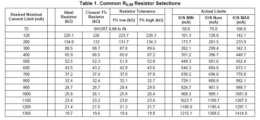
The datasheet recommends two methods of selecting R1013. The first is to use the Current-Limit Threshold vs Rilim curve shown below (from datasheet) to find the intersection of RILIM and the maximum desired load current on the IOS(min) curve and choose a value of RILIM below this value.
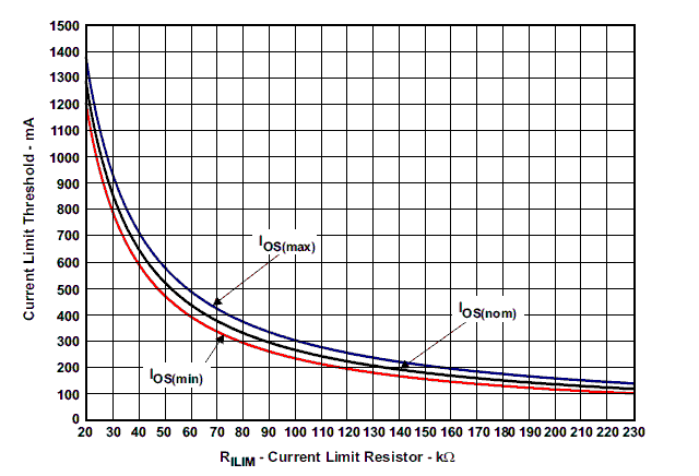
The second method is to use equations below:
Ios(min)(mA)=[25230V/[Rilim]^1.016 (kohm)]
Then we select the closest 1% resistor below the calculated value.
With Ios(min)=500mA, we get Rilim=46.4 kohms which will give us a current limit of: Ios=22980/(Rilim^0.94)=616mA
This value of current is too high for our design, so i used trial and error in conjunction with table 1 shown below (from datasheet). Common Rilim Resistor Selection on the datasheet to come up with a value of Rilim that will get us as close to 500mA as possible (which is by the way the max current the usb should source.)
Rilim=57.5 kohms which yields a 509.6 mA current limit.
Capacitors
C1017
This is the input decoupling capacitor from IN to GND used for local noise decoupling. It reduces ringing on the input due to power supply transients.
This capacitor is 100uF ceramic capacitor which is above the recommended range (>= 0.1uF)
C1018
This capacitor value is a USB requirement. It's an electrolytic capacitor used for electrical noise attenuation between the + 5V Vbus line and OUT pin of U1004.
Value is 100nF.