The generic node is expected to interface with the following peripherals
- USB
- Serial
- SPI
- I2C/TWI
- CAN
- 1-Wire
- Analog inputs
- GPIO
The state of the interface implementations are as follows:
- USB
- Not yet implemented.
- Serial
- Serial port communication is implemented.
- Flow control not yet implemented.
- SPI
- General SPI communications implemented.
- Device specific SPI functions implemented (SCP pressure sensor.)
- I2C/TWI
- Protocol algorithm documented.
- Stub code for Master functions in code repository.
- CAN
- Not yet implemented.
- 1-Wire
- Not yet implemented.
- Analog
- All channels available
- GPIO
- All pins available
- USB
- LV2C:GFE:U2203 TPS63000 Hap Output Regulator
- The HAP output regulator IC (TI TPS63000) takes the voltage supplied by the battery or charger in the HAP and DC-DC converts it to the required voltages for the remainder of the circuit. In most cases this is 3.3V, though with small modifications this voltage can be set to anywhere from 2.5 to 5.5 Volts. C2221 is a simple bulk input capacitor and serves to filter transients spkes and noise from the input power. R2011 and C2222 act in concert to create a time constant that is used to ensure that power is ready to be supplied befre the control circuit begins operation. L2202 is the Inductor used in the output filter of the Buck-Boost supply. R2216 and R2217 create a voltage divider that completes the feedback loop, R2216 is bypassed with capacitor C2223 to provide faster response to transient spikes. R2216 should be set for 1Mohm for operation of the circuit at 3.3Vdc or can be replaced by a 1.8Mohm resistor for the circuit to operate at 5Vdc, though Inductor L1 may need to be resized for this capability to be safely implimented. C2224 is used as the output filter capacitor and fulfills the role of reducing switch noise on the output. The circuit is synchronized to the 1.5MHz clock that is stepped down from the system clock by connection to the PS/Sync pin resulting in constant frequency operation that should not interfere in audio bands. The TPS63000 is noteworthy in that it acts as either a Buck regulator, or a boost regulator and not as an inefficient buck-boost regulator. It manages this by only activating two of it's four internal switches at a given time. The TPS63000 changes automatically from buck to boost operation as required on a per cycle basis.
- LV2C:GFE:U2204 LTC4085 HAP Battery Charger and Power Path Controller
- The HAP battery charger is built around the LTC4085 battery charger IC from Linear Technologies. The LTC4085 is a linear charger that has the capability to control 2 external P-MOS devices while charging the battery. During normal operation power is supplied by the SPS (LV2C:GFE:U2202) and there is no need for the battery. While power is supplied from the SPS The !ACPR! signal from the charger (AC power Present, though in our case the power is DC) will enable power-flow through Q2204 to the HAP Output Regulator (LV2C:GFE:U2003) bypassing the LTC4085. During loss of SPS power, the !ACPR! signal goes away blocking the reverse flow of power from the battery toward the SPS. Anytime the load draws the output voltage down, the ideal diode controller in the LTC4085 will begin to feed power from the battery to the load. This is done both through an internal ideal diode between the BAT and OUT pins, as well as by controlling the gate of Q2205 and using it in parallel with the internal diode. Paralleling the internal diode allows lower resistance sourcing of the battery power to the load. The !CHRG! pin is ground3ed to indicate the battery is charging when the charge current threshhold is passed. Threshhold is at 5000V/Rprog, or 50mA.
- LV2C:GFE:D2202
- Suggested Part: digikey 475-1278-1-ND (OSRAM Semiconductor: LS R976-NR-1-0-20-R18), 0805 package, 2.0Vfwd, 20mA test = 104mcd
- When the battery charge current is above 50mA this LED is lit indicating the battery is charging. The LED is chosen as a red LED since it will be indicating that battery is charging when it is lit. We don't want it to draw a lot of power, so it has been chosen as a 2mA part in an 0805 package. While not bright, it should be useable. The current is set by resistor R2213 to be 2mA when the battery is charging (Vout-Vfwd)/Iset = (4.2V-20V)/2mA = 1100 ohms.
- LV2C:GFE:B2201
- Suggested Part:
- LV2C:GFE:R2207 Rprog
- Suggested Part: digikey (), 100k ohm, 0805 package.
- The value of this resistor sets the charging current to the battery. The voltage across it can also be monitored by the LPC2348 to get an idea of the actual charge rate at any given moment. With Rprog = 100k ohms the charge current is set to 500mA. Ichrg(A)=50,000V/Rprog.
- LV2C:GFE:R2208 Rclprog
- Suggested Part: digikey (), 660 ohm, 0805 package.
- The Current Limit Program resistor sets the input to output current limit. During normal operation and battery backup operation we will not be depending on the input to output current, as it is likely a hiugher voltage drop path than that of Q2204. It is currently set at 1.5A in case Q2204 is not populated on a given board, though that would also require pin 7 (wall) to be grounded. Icl(A)=1000V/Rclprog, Rclprog = 660 ohms for 1.515A max. Voltage on the Clprog pin is always proportional to the current flowing from In to Out and can be calculated by In(A)=(Vclprog/Rclprog)*1000
- LV2C:GFE:R2209 Rnom
- Suggested Part: digikey (), 121k, 1%, 0805 package.
- This resistor forms a voltage divider circuit with the thermistor R2214 and its delta modifying resistor R2215 which results in a voltage dilivered to the NTC pin that represents the current temperature of the battery. As we want the thermistor to use a minimum amount of power in this design, we are using a 100k thermistor. The resistor value is then calculated by: Rnom=((Rcold-Rhot)/(2.815-.4086))*Rntc (where Rntc is 100k @25C and Rcold is 3.363 @0C, Rhot is .3507 @50C (3.363 and .3507 are from the conversion table for the vishay thermistor R2214 <http://www.vishay.com/docs/33011/convtabs.pdf>) resulting in a value of 125k, using the nearest standard 1% resistor results in Rnom = 121k ohms.
- LV2C:GFE:R2211
- Suggested part: 100 Ohms
- Value from Datasheet. In combination with C2222 this resistor creates a time constant that forces the controller to wait for power to be applied to the switches before the controller begins operation.
- LV2C:GFE:R2212 Gate Pull-Up
- Suggested Part: digikey (), 1k ohm, 0805package.
- This resistor is used to pull the gate voltage up to the output voltage when the !ACPR! signal is not present.
- LV2C:GFE:R2213 Diode Current limit
- Suggested Part: digikey (), 1000 Ohms, 0805 package.
- This resistor sets the current through diode D2202. Current flows when the LTC4085 pulls the !CHRG! pin low indicating that the battery is charging. (Vout-Vfwd)/Iset = (4.2V-2.0V)/2mA = 1100 ohms, use 1k as it is still close and should result in only a 2.2mA current draw during use.
- LV2C:GFE:R2214 Thermistor
- Suggested Part: digikey 541-1140-1-ND (Vishay/Dale NTHS0805N17N1003JE)
- This thermistor is an 0805 package with a 100k ohm value at 25C. Rntc is 100k @25C and Rcold is 3.363 @0C, Rhot is 0.3507 @50C (3.363 and .3507 are from the conversion table for the vishay thermistor R2214 <http://www.vishay.com/docs/33011/convtabs.pdf>)
- LV2C:GFE:R2215 R-delta
- Suggested Part: digikey (), 15k, 1%, 0805 package.
- This resistor forms a voltage divider circuit with the thermistor R2214 and bias resistor R2209 which results in a voltage dilivered to the NTC pin that represents the current temperature of the battery. This particular resistor is in series with the thermistor and widens the temperature delta of the thermistor to set 50C as the the T-hot trip point. The resistor value is calculated by: Rdelta=([(.04086/(2.815-.4086))(Rcold-Rhot)]-Rhot)Rntc (where Rntc is 100k @25C and Rcold is 3.363 @0C, Rhot is .3507 @50C (3.363 and .3507 are from the conversion table for the vishay thermistor R2214 <http://www.vishay.com/docs/33011/convtabs.pdf>) resulting in a value of 16k, using the nearest standard 1% resistor results in Rnom = 15k ohms.
- LV2C:GFE:R2216 Feedback Resistor
- Suggested part: 1M ohm resistor for 3.3V operation.
- R2216 calculation (3.3V): 1.12MOhm = R2((Vout/Vfb)-1), Vout = 3.3V, Vfb = 500mV, R2217 = 200kohms
- Suggested part: 1.8M ohms for 5V operation, ensure that L2202 is capable of safe operation at 5Vdc before making this change.
- R2216 calculation (5V): 1.8MOhm = R2((Vout/Vfb)-1), Vout = 5.0V, Vfb = 500mV, R2217 = 200kohms
- LV2C:GFE:R2217 Feedback Resistor
- suggested part: 200k Ohms
- datasheet recommends keeping this part in the range of 200k ohms. No good reason to change this, though the efficiency could be slightly better if a larger value is used. Keep Feedback divider current at or above 1uA.
- LV2C:GFE:C2219 Charge Timer Capacitor
- Suggested Part: digikey (),
- This capacitor sets the duration of the Charge timer for the LTC4085. Ttimer(hours)=(CtimerRprog3hours)/(0.1uF*100k)
- LV2C:GFE:C2220 Bulk Output capacitor
- Suggested Part: digikey (), 4.7uF
- Datasheet recommends at least 4.7uF bypass cap from the OUT pin of the LTC4085 to ground. This capacitor holds up the output voltage when the battery is initially switched in, a job that could possibly be handled by C2221 if it is close enogh to the switches.
- LV2C:GFE:C2221 Bulk Input Capacitor
- Suggested part: 4.7uF, X7R ceramic
- Value is as suggested in Datasheet, recommend small ceramic cap as close to pins as possible.
- LV2C:GFE:C2222
- Suggested part: 0.1uF, X7R ceramic
- Value from datasheet. In combination with R2211 this capacitor creates a time constant that forces the controller to wait for power to be applied to the switches before the controller begins operation.
- LV2C:GFE:C2223 FeedForward Capacitor.
- Suggested part (3.3V): 2pF, X7R ceramic
- C2223(3.3V)= 1.96pF = Feedforward capacitor = 2.2uS/R1
- Suggested part (5.0V): 1.2pF, X7R ceramic
- C2223(5V)= 1.22pF = Feedforward capacitor = 2.2uS/R1
- LV2C:GFE:C2224 Bulk Output Capacitor
- Suggested part: 22uF, X7R ceramic
- C2224(min) = 11uF = Cout=5L(uF/uH), L=2.2uH. In combination with L2202, this capacitor acts as the output filter, datasheet recommends small ceramic cap as close to Vout and Pgnd pins as possible.
- LV2C:GFE:L2202 Filter Inductor
- Suggested Part: Digikey 587-1669-1-ND (Taiyo Yuden NR4018T2R2M), 2.2uH surface mount power inductor.
- Recommended value: 2.2uH, 1.75A Irms, 2.26A Isat
- L2202(suggested) = 2.2uH, this is the inductor value suggested in the datasheet for 3.3V operation.
- L2202(min) = 1.57uH, this is the larger of 1.57uH = (Vout(Vinmax-Vout)/(Vinmaxf0.3A) or 1.34uH = (Vin_min(Vout-Vinmin))/(Vinminf0.3A), where Vout=3.3V, Vinmin=2.5V, Vinmax=4.2V, f=1.5MHz.
- Imax(3.3V) = 1.74A, Isat= 2.26A = Imax+30%
Legacy devices : This category includes much of the front-end protection circuitry (Capstone 2006 Frontend Passive Block) and includes devices that have carried over from the 2006 capstone design, often with few or no changes.
LV2C:GFE:D2203 [Capstone2006 designation: D201] SPS Output Power On LED
- Part Description: 1.9 V, 90 mcd @ 20 mA, 609 nm, 0805, Orange Diffused LED, CML Innovative Technologies Inc, CMDA5BA7D1S (Digi-Key p/n L71515CT-ND $3.00/10) http://www.chml.com/pdf/temp/CMDA5BA7D1S.pdf.
- Purpose: This is an orange LED which is lit given that the nominal SPS 3.3 V rail is up. It is mainly used as an initial indicator of the 3.3 V rail's status. Orange was an arbitrary choice, however any other LEDs in the Glue Logic section needed to be different colors. The intensity and viewing angle are not critical since the only time the information from the LED is useful is in trouble shooting on the ground. It remains lit throughout the whole flight.
- Specifications/ Calculations: From the CMDA5BA7D1S datasheet, Vf = 1.9 V. We specified the LED drive current to be 2 mA. See R2241 for I-V calculations.
- Changes from LV2B to LV2C: Part number only.
- LV2C:GFE:CR2201 [Capstone2006 designation: CR251] SPS Secondary Buck (Catch) Schottky Diode
- Part Description: 30 V, 1.5 A, 4 ns, New MiniPower 2P, Cut Tape, RoHS Compliant???, Panasonic - SSG, MA2Q70500L (Digi-Key p/n MA2Q70500LCT-ND $0.83/1) http://www.semicon.panasonic.co.jp/ds/eng/SKH00017BED.pdf.
- Purpose: CR2201 along with C2252 and L2202 form the second buck switching voltage power regulator which will be eventually regulated down to 5 V possibly with a low-dropout (LDO) linear voltage regulator. For consistency we used the same Schottky diode as CR200. Also the general understanding was that this secondary buck will power specific parts like 5 V ADCs on certain nodes (like the IMU) and we expect that this diode's rated specs are more than enough.
- Specifications/ Calculations: Using the formula on page 9 in the LT1767 datasheet we calculated the average DC current that CR251 should be able to handle. Id,avg = Io (Vin - Vout) / Vin, where Io is the secondary output current of the SPS, Vin is the voltage at the node which is between L200a and L200b and Vout is the SPS secondary output voltage. We assumed that Vin would be switching somewhere between 1.6 V and 7 V. With Vout = 5 V and using the worst case Io = 1 A and Vin = 7 V values Id,avg = 286 mA (again this diode is overrated). We knew that not every node would need a secondary 5 V supply but even the ones that did, the added current should not cause overcurrent events (see U2250). Hopefully.
- Changes from LV2B to LV2C: Part number only. Due to the nature of the new TPS63000, this is unlikely to function. In LV2B this was connected to a simple buck supply and could have worked. In LV2C, it is unlikely to raise the voltage from 3.3 to 5 volts, but it has been left in as it can be depopulated if it turns out to be nonfunctional.
- LV2C:GFE:R2241 [Capstone2006 designation: R214 or R241] 3.3V Output Power On LED Current Limiter Resistor
- Part Description: 649 ohm, 0805, 1%, 1/8 W, Cut Tape, RoHS Compliant, Rohm, MCR10EZHF6490 (Digi-Key p/n RHM649CCT-ND $0.38/10) http://www.rohm.com/products/databook/r/pdf/mcr10.pdf.
- Purpose: R2241 is the SPS Output Power On LED current limiting resistor.
- Specifications/ Calculations: From the datasheet Vf = 1.9 V, resulting in a current limiting resistor of about, R2241 = (3.3 V - 1.9 V) / (2 mA) = 650 ohms. The closest standard value was 649 ohms.
- Changes from LV2B to LV2C: Part number only.
- LV2C:GFE:C2252 [Capstone2006 designation: C252]
- Part Description: TBD
- Purpose: This cap along with C2252A, CR2251 and L2202 form the second buck switching voltage power supply which will be eventually regulated down to 5 V possibly with a low-dropout (LDO) linear voltage regulator. These are application specific caps whose values are mostly independent from the SPS design.
- Specifications/ Calculations: The only difference between C2252 and C2252a are the packages and that only one of them will actually be on the PCB. Since we do not know any details about the actual application specific circuitry each SPS will power from an SPS design point of view, we chose to use both a 0805 and 1206 package. We chose two packages because we moved all relevant parts to the 0805 package from 1206 as in the LV2 SPS design and in case a specific application node needs a more beefy cap a 1206 package cap can be used. The lay out of the parts will not be side by side as suggested in the schematic but are offset and superimposed on top of each other on the same side of the PCB. Because only one cap will be used we offset the pads such that they are not directly on top of each other and either package can be placed down thus saving space. The values are TBD.
- Changes from LV2B to LV2C: Part number only. Due to the nature of the new TPS63000, this is unlikely to function. In LV2B this was connected to a simple buck supply and could have worked. In LV2C, it is unlikely to raise the voltage from 3.3 to 5 volts, but it has been left in as it can be depopulated if it turns out to be nonfunctional.
- LV2C:GFE:C2252A [Capstone2006 designation: C252A]
- Part Description: TBD
- Purpose: This cap along with C2252, CR2251 and L2202 form the second buck switching voltage power supply which will be eventually regulated down to 5 V possibly with a low-dropout (LDO) linear voltage regulator. These are application specific caps whose values are mostly independent from the SPS design.
- Specifications/ Calculations: The only difference between C2252 and C2252a are the packages and that only one of them will actually be on the PCB. Since we do not know any details about the actual application specific circuitry each SPS will power from an SPS design point of view, we chose to use both a 0805 and 1206 package. We chose two packages because we moved all relevant parts to the 0805 package from 1206 as in the LV2 SPS design and in case a specific application node needs a more beefy cap a 1206 package cap can be used. The lay out of the parts will not be side by side as suggested in the schematic but are offset and superimposed on top of each other on the same side of the PCB. Because only one cap will be used we offset the pads such that they are not directly on top of each other and either package can be placed down thus saving space. The values are TBD.
- Changes from LV2B to LV2C: Part number only. Due to the nature of the new TPS63000, this is unlikely to function. In LV2B this was connected to a simple buck supply and could have worked. In LV2C, it is unlikely to raise the voltage from 3.3 to 5 volts, but it has been left in as it can be depopulated if it turns out to be nonfunctional.
The following Eagle schematics represent the initial attempt at schematic capture for the HAP, it is broken into two parts, the charger with battery, and the output regulator.
Two primary contenders for the Li-Ion to 3.3V supply are the LTC3441 from Linear Technologies and the TPS63001 from TI. Both datasheets are linked below.
Linear LTC3441 Datasheet: http://www.linear.com/pc/downloadDocument.do?navId=H0,C1,C1003,C1042,C1116,C1790,P2149,D1054
TI TPS6300X Datasheet: http://focus.ti.com/lit/ds/symlink/tps63000.pdf
Update, the desire for on-chip control via an external thermistor in the battery has been expressed, this removes all existing parts from consideration including the Semtech SC806 IC that was previously chosen. This is a late game catch that results in significant redesign of the charger circuit, but should have little impact overall if the new IC is chosen quickly. To this end there are several ICs from Intersil that look promising. They are :ISL6292, ISL6292D, and the ISL9205. O these the ISL9205 looks most interesting initially.
INTERSIL ISL9205 Datasheet: http://www.intersil.com/data/fn/fn9252.pdf
INTERSIL ISL6292 Datasheet: http://www.intersil.com/data/fn/fn9105.pdf
INTERSIL ISL6292D Datasheet: http://www.intersil.com/data/fn/fn9166.pdf
The SC806 had been chosen for the HAP battery charger and the LTC3441 had been chosen as the HAP output converter.
The datasheet for the Semtech SC806 lithium ion battery charger is here: http://www.semtech.com/pc/downloadDocument.do?navId=H0,C1,C100,C149,P2432&id=623
Component choices for the SC806 Charger are as follows:
- Cin
- 0.1uF
- Value is from the datasheet and is meant to eliminate voltage spikes due to sudden load changes or other issues.
- This bulk capacitor needs to be placed as close to the input as possible.
- Cout
- 0.1uF
- Value is from the datasheet and is meant to eliminate voltage spikes due to sudden load changes or other issues.
- This bulk capacitor needs to be placed as close to the input as possible.
- Rterm
- 5k ohms
- Rterm = (1.5V/Ipchrg) * 100, Ipchrg is the desired precharge current allowable values range from 10mA to 125mA and 30mA has been chosen. This value should include the expected current drain on the battery due to the load, as well as the actual precharge current. This will allow the battery to precharge while still supplying current to the load.
- Rprgm
- 1.5k ohms
- Rprgm = (1.5V/Ifchrg) *1000, where Ifchrg is the fast charge current, which maxes out at 1.0A for this IC. This is the maximum charge rate into the battery, but must be set to include teh expected load current. If the load draws current beyond 1A, the additional current will have to be drawn from a combination of the battery and the SC806.
Battery choices:
model: PL-053048 manufacturer: Batteryspace.com Capacity: 750 mA Dimensions: 1.89 x 1.18 x .197 Datasheet: http://www.batteryspace.com/ProductImages/li-ion/053048.pdf
model: 30124 manufacturer: Tenergy capacity: 450 mA dimensions: 1.65 x .83 x .24 datasheet: http://www.all-battery.com/productimages/lipopacks/3.7V450mah602040.pdf
model: GMB403040 manufacturer: GUANGZHOU MARKYN BATTERY CO., LTD Capacity: 450 mA Dimensions: 1.6 x 1.2 x .16 datasheet: http://www.gmbattery.com/dl/cp11/li-ion/LIPO/BlueTooth/GMB403040.pdf
- LV2C:GFE:U2202 LT3972 Buck Regulator
- The LT3972 is the heart of the SPS regulator. The LT3972 is a switching regulator from Linear Technologies. It can withstand input voltages as high as 62V which minimizes front end protection circuitry. It is synchronized to the 1.5MHz clock coming from the Micro-controller system.
- http://www.linear.com/pc/productDetail.jsp?navId=H0,C1,C1003,C1042,C1032,C1082,P86661
- The main function it performs is dropping the 10-20VDC coming in from the APS down to a more workable 5 volts. Specifically in our case it is set for 5.0V. For nodes without the HAP, the SPS can be reconfigured to run at 3.3VDC directly removing the need for the HAP and it's associated 3.3V output regulator.
- LV2C:GFE:D2201 Catch Diode
- Suggested Diode = Digikey Part number = PDS340DICT-ND, Diodes-Inc PDS340-13, has the following salient details: -- Vreverse = 40Volts , Iave = 3.0Amps , 6.6mm x 3.6mm footprint.
- Alternate Diode = Digikey Part number = MBRA340T3GOSCT-ND , On-Semi MBRA340T3, has the following salient details: -- Vreverse = 40Volts , Iave = 3.0Amps , 6mm x 3mm footprint. Note apparent junction temperature difference and minimum buy compared to PDS340.
- Id(avg) = (1.875,,2.14)A
- Id(avg) = Iout(Vin-Vout)/Vin, Iout=2.5A(max), Vin = (10,,35)V (35V max for IC before shutdown due to OVP), Vout=5V
- Use a Schottky diode, faster is better for efficiency, 40Vmax is fine since the OVP will shutdown the IC from 35V to 62V, beyond that the diode is likely to be the least of the worries, as the LT3972 will have perished.
- LV2C:GFE:D???? Reverse Flow Diode (removed expect Q2250 to handle this job, no need for the extra loss it would introduce.)
- This diode is in place to prevent a shorted input from drawing current in the reverse direction through the SPS and draining the battery. Utilizing the same part as the catch diode.
- Use a Schottky diode, faster is better for fault protection, 40Vmax is overkill as the battery has a maximum voltage below 5Vdc, but is good for protection against a reversed input as well. Ideally this diode should create as little voltage drop as possible in the forward direction to minimize impact to operating efficiency.
- LV2C:GFE:R2202 Frequency Set Resistor Rt
- 26.7k Ohms
- When Sync to 1.5MHz is desired, use the table value for 1.5MHz - 20%, or 1.2MHz.
- For simulation use 20.2k ohms as this results in an operating frequency of 1.49MHz.
- This resistor is not used or present in the final design (therefore no part number) the pin is connected to a clock for sync.
- LV2C:GFE:R2204 Soft Start Resistor
- 500k ohms
- Works in combination with the Soft Start Capacitor below.
- LV2C:GFE:R2205 Feedback resistor R1
- suggested Resistor: Digikey Part Number = RHM536KCCT-ND, Rohm = MCR10EZHF5363, 536kOhm, 1%, 0805, thick film.
- 532.911k ohms, use 532k ohms.
- R1=R2((Vout/0.79V)-1 , where R2=100kohms, Vout=5Volts (chosen as Vin for the Charger of the HAP)
- Could use 560k, but then R2 has to be 105k ohms.
- LV2C:GFE:R2206 Feedback resistor
- 100k ohms
- This component value was chosen from the reference design.
- It needs to be big enough to draw very little current through the feedback loop and still feed the appropriate voltages to the feedback error amp and the power good error amp.
- LV2C:GFE:C2201 Input Capacitor Cin1 (OK to place slightly further from the IC)
- Per Tim, using a physically large 10uF is fine, but then add a physically small 1uF cap in very close.
- Suggested Capacitor = Digikey Part Number = 587-2247-1-ND , Taiyo Yuden = UMK325BJ106KM-T , 10uF , 50Volt, 20% , Ceramic , 1210 , X5R
- LV2C:GFE:C2202 Input Capacitor Cin2 (Place as close to the IC as possible)
- Suggested Capacitor : Digikey Part Number = 490-3909-1-ND , Murata = GRM31CR72A105KA01L , 1uF , 100Volt, 10% , Ceramic , 1206 , X7R
- 15uF (could be in range of (10,,20)uF)
- Xc = -j.01 ohms = 1/jwc , w = 2pi * 1.5MHz, c=10uF
- So long as Xc is small at the switching frequency this cap will work, any cap in the range is fine, but the smaller they are the closer they need to be to the IC and the catch diode in order to effectively handle the EMI from the switching.
- Watch out for Ringing during hot plugging, the cap needs to be able to withstand the full 62V that the LT3972 can during faults and plug in ringing.
- Use types X5R and X7R, DO NOT USE type Y5V!! (warning per data-sheet)
- LV2C:GFE:C2203 Frequency Compensation Capacitor
- Suggested Capacitor = Digikey Part Number = PCC681BNCT-ND , Panasonic-ECG = ECU-V1H681KBN , 680pF , 50V , package = 0805.
- Chosen as 15k ohms and 680pF from the reference schematic and the data-sheet.
- Need help figuring these out.
- LV2C:GFE:C2204 Boost and Bias Capacitor
- Suggested Capacitor = Digikey Part Number = PCC1832CT-ND , Panasonic-ECG = ECJ-2YB1E224K , 0.22uF, 25V , package = 0805.
- 0.22uF
- This is set at 0.22uF per figure 5A in the data sheet. So long as the input voltage remains above 7.5V the boost/bias considerations appear minimal as there should be plenty of voltage available to successfully start the IC.
- LV2C:GFE:C2205 Output Capacitor
- Suggested Capacitor = Digikey Part Number = 587-2086-1-ND , Taiyo Yuden = TMK325BJ226MM-T , 22uF , 25Volt, 20% , Ceramic , 1210 package , X5R (Use of this part allows for a shorted switch and is the same part as the suggested input capacitor which is available through Digikey in lots of 10)
- Alternate Capacitor = Digikey Part Number = 445-3945-1-ND , TDK = C3225X7R1C226K , 22uF , 16Volt, 10% , Ceramic , 3.2mm x 2.5mm , X7R
- Alternate Capacitor = Digikey Part Number = 478-4594-1-ND , AVX = 1210YC226MAT2A , 22uF , 16Volt, 20% , Ceramic , 3.2mm x 2.5mm , X7R
- 13.3uF minimum
- Cout = 100/(Vout*f(sw)), Vout=5V, f(sw)=1.5MHz
- Ensure that ESR is as low as possible to maximize efficiency (0.05 ohms or less)
- Look for High performance electrolytic or Tantalum caps
- Try to use type X5R or X7R
- LV2C:GFE:C2225 Soft Start Capacitor
- Suggested Capacitor = Digikey Part Number = PCC1840CT-ND , Panasonic-ECG = ECJ-2YB1H104K , 0.1uF, 50V , package = 0805.
- Choose a large RC time constant to minimize voltage overshoot and reduce Imax for the switch at startup. Choose resistor to supply 20uA when RUN/SS is at 2.5V.
- Want (3.75k, 585k, 875k) ohms for Vin = (10,14.2,20). 500k worked fine in LT-Spice and is the value chosen. As for the cap, it shows .22uF on the reference design, but won't run the system with that value in LT-spice, choosing 0.1uF as in the test fixture for the LT3972 works fine in the simulation and is the chosen cap value.
- LV2C:GFE:L2201 Inductor
- Suggested Inductor = Digikey Part number = 513-156-1-ND, Coiltronics DR74-6R8-R, has the following salient details: -- 6.8uH, Irms = 2.60Amps , Isat = 3.67Amps , DCR = 0.0418Ohms , Shielded , 8mm x 8mm x 4.25mm , Surface Mount.
- 5.9uH min
- Per data-sheet, start with di/dt for L and use dI= 1A = 0.4(Ioutmax) , Ioutmax=2.5A
- Ipeak must be lower than Ilim (the switch current limit)
- I(L-peak)= 3A = Ioutmax + dI/2 , Ioutmax = 2.5A, dI = 1A
- This is good as Ilim ranges from (5.5A to 4.5A) and is always greater than 3A.
- check ==> Ioutmax = Ilim-dI/2 = 4A , Ilim(worst case) = 4.5A, dI = 1A, So Ioutmax is at worst 4A, resulting in a value that is still above 3A, this is good.
- Largest dI occurs at max Vin, choose L using the following formula:
- L=[(Vout+Vd)/(FswdI)][1-((Vout+Vd)/Vinmax)], Vout=5V, Vd=0.4V, Fsw=1.5MHz, dI=1A, VinMax = 20V (possibly 30V during failures?)
- L=5.2uH for Vin = 20V, or L=5.9uH for Vin = 30V
- Larger values are OK as they will only make dI smaller resulting in improved system responses.
- RMS rating of L must be greater than Imax = 2.5A
- Saturation current should be about 30% higher, Isat = 3.25A, but want Isat above 5A during startup, shorts, Over Voltages, and other failures.
- To keep efficiency high, DCR should be kept below 0.1 ohm.
- To minimize EMI, use a shielded toroid with a ferrite core.
- Again, larger L is good since they should have better DCR values, smaller ripple current (dI), and an easier time keeping out of discontinuous mode, but the physical size will be a limiting factor.
- Legacy devices : This category includes much of the front-end protection circuitry (Capstone 2006 Frontend Passive Block) and includes devices that have carried over from the 2006 capstone design, often with few or no changes.
- LV2C:GFE:U2250 [Capstone2006 designation: U250]
- Part Description: MAX5902AAETT +72 V, SOT-23, Simple Swapper How-Swap Controller. Ordered samples from vendor, no Digi-Key. http://pdfserv.maxim-ic.com/en/ds/MAX5902-MAX5903.pdf.
- Purpose: This hot-swap controller IC serves two purposes: (1) circuit-breaker and (2) the first stage of UVLO protection. The version we chose had a input voltage range of +9 V to +72 V, a 300 mV circuit-breaker threshold voltage, limited inrush current ("soft start") and was an automatic retry circuit-breaker. It also had a built-in thermal shutdown and active low power good (!PGOOD) indicator output pin. The device needed a UVLO resistor divider network (R2250, R2251) and an external PMOSFET (Q2250) switch. There are four events which will cause Q250 to turn off: (1) if there is undervoltage at the input, (2) if there is overcurrent, (3) if the die temperature exceeds +125 C and (4) the ON/!OFF pin 6 is forced low for at least 10 ms. See the MAX5902 datasheet.
- Specifications/ Calculations: The reasons we chose the 300 mV automatic retry circuit breaker version was that we wanted the SPS to be able to recover from a fault condition by itself and we expect that the nominal load current will not be very close to the 400 mA maximum limit but closer to 300 mA or less. Hence steady-state currents in the range of 400 mA to 500 mA qualify as an overcurrent event and should be detected. To avoid wasting power dissipated by Q220's RDS(on) and R2252, those values should be kept low, therefore the voltage across them should also be low and the 300 mV threshold version satisfied that. Upon power up U2250 keeps Q2250 off and if trigger events (1) and (2) are non-existent, then it gradually turns Q2250 on to saturation in approximately 150 ms. The drain of Q2250 is gradually enhanced at a rate of about 9 V/ ms. This start sequence limits the inrush current giving some "soft-start" protection to its load. Once all transients are gone before the 150ms time period and Q2250 is fully saturated, U2250's circuit-breaker functionality comes up and monitors the Vds of Q2250 between pins 1 and 2. Before this initial power up 150 ms period there is no circuit-breaker functionality. If any one of the 4 trigger events occurs U2250 will turn Q2250 off, de-assert !PGOOD (output a logic high) and reinitiate the start sequence given that the trigger event(s) disappears during the 150 ms period, if not the 150 ms period will repeat. There are two typical turn off times regarding Q2250: 10 ms and 4 us. If there is an ON/!OFF or UVLO trigger event, they need to exist for 10 ms before U2250 turns Q2250 off, which will take an unspecified amount of time. If there is an overcurrent or temperature trigger event, then Q2250 is turned off in 4 us. If the trigger events disappear after Q2250 turns off within 150 ms, then the normal start sequence is reinitiated. Since the purpose of U2250 was to be a circuit-breaker we decided not to use the ON/!OFF pin to turn Q2250 off via any SPS feedback. Only an UVLO condition would be a trigger event. The UVLO threshold was specified as 9 V. See R2250 and R2251. This meant that when a trigger event other than a UVLO condition happens, U2520 would turn Q2250 off in 4 us and would reinitiate the start sequence after a trigger event free 150 ms time period. We needed a way for the LPC2368 (U2201) microcontroller to turn off the SPS, so we connected a logic level NMOSFET (Q2282) to a GPIO pin and connected the drain of Q2282 to the ON/!OFF pin of U2250. Also we connected the active low !PGOOD pin to another GPIO pin for monitoring and/or interrupt purposes. See the GLUE Logic section regarding U2280 and Q2282. See R2253 and Q2251 for the "overvoltage to overcurrent" trigger event emulation. One bad thing that we did not like was the relatively high supply current of U2250 being 1 mA to 2 mA. We believe that U2250 will draw the most current from the power bus when the SPS is in a standby/shutdown mode. NOTE: According to the MAX5902 datasheet there are multiple package options for the different versions of the MAX5902: a TDFN and SOT23 package. All SOT23 packages have the specification that, "This device is constructed using a unique set of packaging techniques that impose a limit on the thermal profile the device can be exposed to during board level solder attach and rework. This limit permits only the use of solder profiles recommended in the industry standard specification, JEDEC 020A, paragraph 7.6, Table 3 for IR/VPR and convection reflow. Preheating is required. Hand or wave soldering is not allowed.", which may or may not present a problem.
- changes from LV2B to LV2C: Part number only. Part must still be ordered outside of digikey (vendor still shows samples in stock)
- LV2C:GFE:U2251 [Capstone2006 designation: U251]
- Undervoltage/Overvoltage Protection (U2251)
- Part Description: Nanopower Push-Pull Output Comparator with Voltage Reference, 1.8 V < Vin < 5.5 V, SOT-23-6, Tape & Reel (TR), RoHS Compliant, Texas Instruments, TLV3012AIDBVT (Digi-Key p/n 296-16830-2-ND $262.50/2250) NOTE: Ordered samples from vendor no Digi-Key. http://focus.ti.com/lit/ds/symlink/tlv3012.pdf.
- Purpose: This comparator compares the specified divided SPS output voltage (see R2254, R2255) to its internal reference voltage (1.242 V) for an overvoltage trigger event at the SPS output. It is powered by a secondary supply consisting of CR2250 and C2250. Also it has a pseudo low-pass filter consisting of C2251 and its output (pin 1) with the input being pin IN+ (pin 3). See CR2250, C2250 and C2251 respectively.
- Specifications/ Calculations: We wanted a low power push-pull output comparator to get rail to rail output swing (approximately 200 mV to 3.1 V) and have reasonable switching and rise/fall times, on the order of several microseconds and nanoseconds respectively. We tied the IN- pin (pin 4) to the internal reference voltage REF pin (pin 5) which will be compared to the divided SPS output voltage at its IN+ pin (pin 3). See R254, R255 and C2251. The "undervoltage" protection is actually provided by CR2250 and C2250 where U2251 will remain powered for a specified amount of time if the +3.3 V SPS output rail drops. See CR2250 and C2250.
- changes from LV2B to LV2C: Part number only, order from vendor, not Digikey.
- LV2C:GFE:CR2250 [Capstone2006 designation: CR250]
- TLV3012AIDBVT "Secondary Power Supply" Schottky Diode (CR2250)
- Part Description: 30 V, 1.5 A, 4 ns, New MiniPower 2P, Cut Tape, RoHS Compliant???, Panasonic - SSG, MA2Q70500L (Digi-Key p/n MA2Q70500LCT-ND $0.83/1) http://www.semicon.panasonic.co.jp/ds/eng/SKH00017BED.pdf.
- Purpose: CR2250 and C2250 form U2251's power supply. This diode prevents C2250 from discharging anywhere but to the V+ supply pin of U2251. U2251 is indirectly powered by the +3.3 V SPS rail. Pin 6 (V+) of U2251 will be charged to a value very close to the +3.3 V SPS rail. As U2251 draws more current when needed and its V+ voltage drops CR2250's Vf below the SPS voltage CR2250 will re-charge C2250. Therefore the average DC current through CR2250 is not easily calculable but will be on the order of tens to hundreds of uA. Schottky diodes were chosen for their fast switching and reverse recovery times. In response to a overvoltage event at the +3.3 V SPS output, U2251 will output a logic high and turn Q2251 on which will cause an overcurrent event at U2250 which will in response turn Q2250 off thus circuit breaking the bus rail from the SPS and the +3.3 V SPS output voltage rail will go to zero. That is the sequence of events without delay times. This is the way U2251 emulates an overcurrent event from an overvoltage event.
- Specifications/ Calculations: CR2250 has a low forward voltage and U2251 has an input voltage supply range of 1.8 V to 5.0 V so when the SPS voltage is being brought up C2250 is being charged through CR2250 leaving the voltage of SPS minus the Vf of CR2250 at pin 6 (V+) of U2251: V+ = 3.3 V - 0.05 V = 3.25 V (approximately). See the first graph on page 2 of the MA2Q705 datasheet given that the steady state nominal forward current through CR2250 < 1 mA. See C2250.
- changes from LV2B to LV2C: Part number only, this is another digikey non-stock part. It will have to be respecified or ordered from another vendor.
- LV2C:GFE:Q2250 [Capstone2006 designation: Q250]
- Part Description: -60 V, -3 A, SOT-23-6, P-Channel MOSFET, Cut Tape, RoHS Compliant, Zetex Inc, ZXMP6A17E6TA (Digi-Key p/n ZXMP6A17E6CT-ND $0.75/1) http://www.zetex.com/3.0/pdf/ZXMP6A17E6.pdf.
- Purpose: This is the external PMOSFET of U2250 which will turn off given that there is one or more of the four trigger events as described earlier. See U2250. U2250 uses the RDS(on) of the saturated Q2250 as a current sense resistor which generates a Vds voltage which is detected across the Vs (Pin 1) and DRAIN (Pin 2) pins and if it is greater than some threshold voltage, U2250 will switch Q2250 off thus breaking the circuit.
- Specifications/ Calculations: The maximum SPS output current specified was 400 mA. There are three circuit-breaker threshold voltage versions of U2250: 300 mV, 400 mV and 500 mV. For certain reasons the 300 mV threshold part was chosen. See U2250. Therefore the RDS(on) of the PMOS should be around 300 mV / 400 mA = 0.75 ohm. We used a value of 1 ohm. See R2252. Even though the PMOS is used as a switch (cutoff and saturation) and not an amplifier (cutoff, triode and saturation) we wanted to remove dependence of U2250's threshold voltage detection from the less precise RDS(on) of Q2250 and to a more precise sense resistor. Therefore we added a current sense resistor (R2252) in series with the drain of Q2250 to produce a circuit-breaker resistor, Rcb, which is the series combination of Q2250's RDS(on) and R2252 between the two pins 1 and 2 of U2250. We chose a PMOS with a low RDS(on) compared to the needed calculated value needed to trip the circuit-breaker thereby making R2252 close to Rcb in value. Therefore Q2250 is used mostly as a switch and the voltage drop across R2252 is used to trigger the switch. See R2252. The breakdown voltage of Q2250 has to be greater than 20 V and should have a low "turn on" capacitance. We do not care so much about the Vt but it does affect the "turn on" capacitance but these factors were not considered.
- changes from LV2B to LV2C: Part number only. Price has gone down slightly at digikey to $0.75
- LV2C:GFE:Q2251 [Capstone2006 designation: Q251]
- Part Description: 100 V, 170 mA, RDS(on) = 10 ohm @ Vgs = 4.5V, SOT-23, Cut Tape, RoHS Compliant???, N-Channel Logic-Level MOSFET, Infineon Technologies, BSS123E6327 (Digi-Key p/n BSS123INCT-ND $0.36/1) http://rocky.digikey.com/WebLib/Infineon/Web%20Data/BSS123.pdf.
- Purpose: This is a logic-level NMOSFET. When an overvoltage at the +3.3 V SPS output occurs, U251 will output a logic high turning Q251 on and thus conducting current through R253. The current flowing through R253 also flows through Rcb and its magnitude is dependent on the value of R253 and the bus voltage at the time (nominal value of 16.8 V). When there is no overvoltage at the +3.3 V SPS output U251 outputs a logic low thus keeping Q251 off.
- Specifications/ Calculations: Since the gate of this FET would be driven by the output of a comparator in U251 it would be best for the FET to be a logic-level device. Other concerns was for the drain-source breakdown voltage to be higher than 30 V as the highest possible DC value the bus voltage rail would be is 20 V.
- changes from LV2B to LV2C: Part number only. Original Part is non-stock, call to order at digikey. Should be re-sourced re-specified, or ordered as a vendor sample.
- LV2C:GFE:Q2282 [Capstone2006 designation: Q282]
- Part Description: Logic level N-channel mosfet, 100V, SOT23, Fairchild p/n: BSS123 (Digikey p/n: BSS123NCT-ND $0.29/1)
- Purpose: This Nmosfet allows a Microcontroller GPIO pin to activate the shutoff of U2250 (circuit-breaker) resulting in a disconnection of the APS supply to the SPS.
- Specifications/calculations: See the GLUE logic section of Capstone2006 for detailed explanation of this part.
- changes from LV2B to LV2C: Part number only. Still available through Digikey.
- LV2C:GFE:TVS2201 [Capstone2006 designation: TVS200]
- Part Description: 18 V, SMB, Unidirectional, Cut Tape, RoHS Non-Compliant, Diodes Inc, SMBJ18A-13 (Digi-Key p/n SMBJ18ADICT-ND $0.89/1) http://www.diodes.com/datasheets/ds19002.pdf.
- Purpose: A transient voltage suppressor (TVS), this "zener like" diode protects the SPS (specifically U2202) in the event of an overvoltage at the input.
- Specifications/ Calculations: It should have a breakdown voltage of about 20 V (unlikely maximum bus voltage) and a current carrying capacity greater than the fuse rated current. It should have a fast response time and be unidirectional. In the event of a sustained overvoltage at the input the only allowable part which can be destroyed is the fuse, F200. That is what we want.
- changes from LV2B to LV2C: Part number. The original capstone2006 part is no longer available in digikey. Respecify or find new vendor. One suggested replacement is B72500D200A60V7 (Digikey p/n: 495-3413-1-ND $0.20/1) http://www.epcos.com/inf/75/ds/cd_standard.pdf This is a simple Zener type ESD suppressor in an 0603 package.
- Another replacement possibility is: V2F118C400Y1FDP, digikey p/n:478-2486-1-ND. The difficulty here is that new replacement doesn't handle the current that we are looking for, it maxes out at 1A and would blow before the fuse.
- A final possibility, as the LT3907 is capable of withstanding up to 62V, it could be argued to simply not populate this part, though some ESD protection would be nice.
- LV2C:GFE:F2201 [Capstone2006 designation: F201] Node Power Supply Fuse
- Part Description: 2000 mA, 63 V, 1206, Fast Acting Short Time Lag, RoHS Compliant, TYCO Electronics, 1206SFF200F/63-2 (Digi-Key p/n 1206SFF200F/63CT-ND $0.46/1) http://documents.tycoelectronics.com/commerce/DocumentDelivery/DDEController?Action=srchrtrv&DocNm=SCD25801&DocType=CD&DocLang=EN
- Purpose: This fuse protects the SPS from currents greater than 2000 mA. Its direct purpose however is to protect the power bus from a short circuit fault on the SPS side.
- Specifications/ Calculations: Since the specified maximum SPS current is 2000 mA we chose a fuse rated at 2000 mA. The opening time for the fuse according to its datasheet is .05 s at a current of 8 A, or 5 s at 5 A. Currents of 2 A or below are 4 hours minimum, therefore this fuse will only protect the SPS or power bus from gross currents due to some fault on either side (power bus or SPS) and not to keep the SPS output current within spec, that is U250's job.
- changes from LV2B to LV2C: Part number. New value reflecting the higher current rating of the updated SPS.
- LV2C:GFE:R2218 [Capstone2006 designation: R215] Chassis Ground to Node Ground isolation resistor
- Part Description: 100 kohm, 0805, 1%, 1/8 W, Cut Tape, RoHS Compliant, Rohm, MCR10EZHF1003 (Digi-Key p/n RHM100KCCT-ND $0.38/10) http://www.rohm.com/products/databook/r/pdf/mcr10.pdf.
- Purpose: R2218 provides a DC path from the SPS ground to chassis ground. See page 29 of the CAN Node Switch Mode Power Supply (SPS) (200) section in the Component Design for LV2 Power Electronics (Except Main Battery) engineering design notes.
- Specifications/ Calculations: 100 kohm worked.
- changes from LV2B to LV2C: Part number only. No recognized need for other changes.
- LV2C:GFE:R2250 [Capstone2006 designation: R250]
- Part Description: 61.9 kohm, 0805, 1%, 1/8 W, Cut Tape, RoHS Compliant???, Rohm, MCR10EZHF6192 (Digi-Key p/n RHM61.9KCCT-ND $0.38/10) http://www.rohm.com/products/databook/r/pdf/mcr10.pdf.
- Purpose: R2250 is part of the UVLO resistor divider of U2250.
- Specifications/ Calculations: The UVLO voltage was specified to be 9 V. See page 8 and Figure 3 in the MAX5902 datasheet. Letting R251 = 10.0 kohm and using the typical value of Von/!off = 1.26 V, the UVLO formula from page 8 in the datasheet is R250 = R251 * ((VUVLO / (Von/!off)) - 1) = 61.4 kohm. The closet standard value was 61.9 kohm.
- changes from LV2B to LV2C: Part number only.
- LV2C:GFE:R2251 [Capstone2006 designation: R251]
- Part Description: 10.0 kohm, 0805, 1%, 1/8 W, Cut Tape, RoHS Compliant???, Rohm, MCR10EZHF1002 (Digi-Key p/n RHM10.0KCCT-ND $0.38/10) http://www.rohm.com/products/databook/r/pdf/mcr10.pdf.
- Purpose: R2251 is part of the UVLO resistor divider of U2250.
- Specifications/ Calculations: R251 was specified to be 10.0 kohm. See page 8 and Figure 3 in the MAX5902 datasheet.
- changes from LV2B to LV2C: Part number only.
- LV2C:GFE:R2252 [Capstone2006 designation: R252]
- Part Description: 0.82 ohm, 0805, 1%, 1/8 W, Cut Tape, RoHS Compliant???, Panasonic - ECG, ERJ-6RQFR82V (Digi-Key p/n P.82DCT-ND $2.10/10) http://www.panasonic.com/industrial/components/pdf/AOA0000CE3.pdf.
- Purpose: This resistor dominates the circuit-breaker resistor's (Rcb) value. It is in series with the drain (hence RDS(on) of Q2250 to make up Rcb. The voltage drop across it is used to detect an overcurrent event given that it is greater than 300 mV. See Q2250 and U2250. Note: This value may change due to board level testing results.
- Specifications/ Calculations: Since the typical value of RDS(on) of Q2250 is 0.125 ohm and Rcb was about equal to 1 ohm, R2252 = Rcb - RDS(on) = 0.875 ohm. The closet standard value was 0.82 ohm. Given this value of Rcb and the circuit-breaker trip threshold voltage of 300 mV, the maximum SPS current which can be drawn before an overcurrent event is Imax = 300 mV / (0.125 ohm + 0.82 ohm) = 317 mA which is under the specified maximum SPS current spec.
- changes from LV2B to LV2C: Part number only. Probably need to recalculate the default value, but it is likely to be changed during board level testing regardless.
- LV2C:GFE:R2253 [Capstone2006 designation: R253]
- Part Description: 47.0 kohm, 0805, 1%, 1/8 W, Cut Tape, RoHS Compliant???, Rohm, MCR10EZHF4702 (Digi-Key p/n RHM47.0KCCT-ND $0.38/10) http://www.rohm.com/products/databook/r/pdf/mcr10.pdf.
- Purpose: R253 along with Q2251 will "emulate" an overcurrent trigger event as seen by U2250 when an overvoltage at the SPS output trigger event as seen by U2251 occurs. See Q2251. When the SPS +3.3 V output rises above a certain threshold, the output of U2251 goes high, turning Q2251 on. When this happens it pulls pin 2 of U2250 very close to ground and current flows through R253 and Q251. Now that pin 2 is close to ground and pin 1 is normally close to the power bus voltage this is much greater than 300 mV this causing an overcurrent trigger event for U2250. R2253 limits the extra current pulled through Q2251 when it is turned on.
- Specifications/ Calculations: In normal SPS operation, the voltage drop across Rcb will be less than 300 mV and R2253 is connected to the high impedance pin 2 of U2250 so no current flows through it. If there is an overvoltage trigger event at the SPS output, Q2251 is turned on conducting current through R2253 which will have a voltage drop of approximately 300 mV less than the power bus voltage: VR2253 = 16.8 V - 300 mV = 16.5 V. This results in a current boost of about IR2253 = 16.5 V / 47 kohm = 351 uA which is negligible.
- changes from LV2B to LV2C: Part number only.
- LV2C:GFE:R2254 [Capstone2006 designation: R254]
- TLV3012AIDBVT UVLO Lockout Resistor Network (R254, R255)
- Part Description: 18.2 kohm, 0805, 1%, 1/8 W, Cut Tape, RoHS Compliant???, Rohm, MCR10EZHF1822 (Digi-Key p/n RHM18.2KCCT-ND $0.38/10) http://www.rohm.com/products/databook/r/pdf/mcr10.pdf.
- Purpose: R254 along with R255 form a voltage divider with respect to the +3.3 V SPS output rail. When there is an overvoltage at the +3.3 V SPS output the voltage at the IN- pin (pin 4) of U2251 will be greater than the internal reference voltage of U2251 (typically 1.242 V) and will result in the comparator in U2251 outputing a logic high value. When the SPS output is below a certain threshold the input voltage (pin 4) to U2251 is less than the internal reference voltage and the comparator's output is a logic low.
- Specifications/ Calculations: From the LPC2148 datasheet the maximum supply voltage it can handle is 3.6 V therefore we specified that if the +3.3 V SPS output was to reach 3.5 V we would want this to qualify as an overvoltage trigger event. Since we have been using several 10.0 kohm resistors we specified R255 to be 10.0 kohm. Therefore using the overvoltage trigger event value to be 3.5 V and the compared voltage to be 1.242 V we solved for R254: 1.242 V = (3.5 V * R255)/ (R255 + R254) and solving for R254 = 18.18 kohm. The closet standard value was 18.2 kohm.
- changes from LV2B to LV2C: Part number only, though this is a non-stock digikey part, it should be easy to locate alternate sources, need new value for 5.0V sps rail.
- LV2C:GFE:R2255 [Capstone2006 designation: R255]
- Part Description: 10.0 kohm, 0805, 1%, 1/8 W, Cut Tape, RoHS Compliant???, Rohm, MCR10EZHF1002 (Digi-Key p/n RHM10.0KCCT-ND $0.38/10) http://www.rohm.com/products/databook/r/pdf/mcr10.pdf.
- Purpose: R255 along with R254 form a voltage divider with respect to the +3.3 V SPS output rail. When there is an overvoltage at the +3.3 V SPS output the voltage at the IN- pin (pin 4) of U2251 will be greater than the internal reference voltage of U2251 (typically 1.242 V) and will result in the comparator in U2251 outputing a logic high value. When the SPS output is below a certain threshold the input voltage (pin 4) to U2251 is less than the internal reference voltage and the comparator's output is a logic low.
- Specifications/ Calculations: We specified R255 = 10.0 kohm. See R254.
- changes from LV2B to LV2C: Part number only, need to recalc value for new sps rail at 5.0V
- LV2C:GFE:C2206 [Capstone2006 designation: C203] Node Power Supply Filter Capacitor
- Part Description: 22 uF, 25 V, Tant, T491 Series, 7343-31 (EIA), Cut Tape, RoHS Compliant???, Kemet, T491D226K025AT (Digi-Key p/n 399-3782-1-ND $0.65/1) http://www.kemet.com/kemet/web/homepage/kechome.nsf/vapubfiles/F3102T491.pdf/$file/F3102T491.pdf.
- Purpose: C203 acts as a noise filter between the power bus and SPS. It also serves as a local energy storage node.
- Specifications/ Calculations: It needs to have a voltage rating greater than 20 V and a low equivalent series resistance (ESR) thus a tantalum capacitor was chosen due to their low ESR at a higher capacitance.
- changes from LV2B to LV2C: Part number only. No recognized need for other changes, though the voltage rating is a bit low.
- LV2C:GFE:C2207 [Capstone2006 designation: C204]
- Part Description: 0.33 uF, 50 V, 0805, X7R, Cut Tape, RoHS Compliant, Murata Electronics North America , GRM219R71H334KA88D (Digi-Key p/n 490-3327-1-ND $3.09/10) http://search.murata.co.jp/Ceramy/image/img/PDF/ENG/GRM219R71H334KA88.pdf.
- Purpose: C2207 is a high frequency noise filter between the power bus and SPS. It did not have to have as high a capacitance as C2206 so the trade off was to get a lower value at a low ESR.
- Specifications/ Calculations: It needs to have a voltage rating greater than 20 V and the capacitance value was not very critical but should be much lower than C2206.
- changes from LV2B to LV2C: Part number only. No recognized need for other changes, though the voltage rating is a bit low.
- LV2C:GFE:C2250 [Capstone2006 designation: C250]
- TLV3012AIDBVT "Secondary Power Supply" Cap (C2250)
- Part Description: 2.7 uF, 10 V, 0805, X5R, Cut Tape, RoHS Compliant, Kemet, C0805C275K8PACTU (Digi-Key p/n 399-3127-1-ND $7.02/10) http://www.kemet.com/kemet/web/homepage/kechome.nsf/vapubfiles/F3102X5R.pdf/$file/F3102X5R.pdf.
- Purpose: Along with CR2250, C2250 forms the power supply for U2251. C2250 is charged to a voltage less a forward diode drop (see CR2250) from the +3.3 V SPS output rail under normal operating conditions. U2251 draws a constant 2.8 uA supply current so CR2250 is always trickle charging C2250, therefore the voltage across C2250 will be VfCR2250 = 0.37 V (this is worst case Vf) less than 3.3 V. See CR2250. However U2251 can operate from 1.8 V to 5.0 V. Since the voltage at V+ of U2251 is approximately 3.0 V and the lower limit of the supply voltage range of U2251 is 1.8 V, C2250 has to be able to store enough charge such that if the SPS output drops down by a certain amount of voltage, U2251 is still powered for a certain amount of time thus preventing U2251 from power cycling if the SPS output ramps back up to +3.3 V. We want to prevent this because as U2251 is powering up the comparator could possibly switch. That behavior has to be observed in experiment but we assume that the initial state of the comparator will be logic low. If the SPS output toggles or drops in value we want U2251 to have power for a specified amount of time in case the magnitude of the voltage change of a transient causes a trigger event but lasts a very short amount of time or would normally shut down U2251, thus avoiding the time needed for U2251 to power cycle. When the overvoltage at the SPS output event occurs there is a finite amount of time required before Q2250 is eventually turned off namely the propagation delay of the comparator in U2251, the turn-on delay time of Q2251, the time to turn off Q2250 by U2250 and the turn-off delay time of Q2250. These typical times as are 12 us, 8 ns, 4 us and 26.2 ns as specified on pages 3, 3, 8 and 4 in the TLV3012, BSS1223, MAX5902 and ZXMP6A17E6 datasheets respectively, resulting in an ideal propagation delay of about 17 us. After these propagation delay times, Q2250 is off and the input voltage Vin (pin 2) of U200 is zero volts (after C201 is discharged) triggering the SHDN\ pin and turning off U200. When this happens the power supply to U2251 is essentially removed, so the time constant for C2250 has to be long enough such that as U2250 is going through its start sequence (150 ms) the comparator in U2251 can output a logic low and turn Q2251 off as the voltage it is comparing, IN+ (pin 3), to its internal reference voltage, REF, is the divided (see R254, R255) SPS output rail voltage which at this time is zero volts. To make sure that this sequence of events happen we specified U2251 to have power long enough to turn Q2251 back off while U2250 is turning back on again. Under normal operating conditions (no UVLO event) and assuming that there are no long or catastrophic transients, U2251 should always be on. This design will always keep U2250 on which will minimize any unknown states at the comparator output resulting from U2251 turning off, then on again, etc. Upon initial power up we assume that the output of U2251 will be logic low keeping Q2251 off to prevent a false overcurrent event for U2250 which may prevent the SPS from working as U2250 will never turn Q2250 on and will just cycle. This seems unlikely because upon initial power up, U2251 has no power and cannot output logic high. However as the +3.3 V SPS output is being brought up the output of the comparator is undefined which is not good being directly connected to the gate of Q2251 but we still think that Q2251 will remain off or will rapidly switch off if it is ever on after the transients.
- Specifications/ Calculations: We calculated the needed amount of charge, Qt, C2250 would have to store such that U2251 would have power for at least 0.5 s (our specified amount of time U2251 should have power during these events) given that the SPS output voltage dropped by 1 V from which we calculated C2250's capacitance. C2250 = [((Qt * 1.2) + (Iq * tp))] / Vp, where Qt = [((Input Capacitance) * Vt) + ((Reverse Transfer Capacitance) * Vin)], Iq = 2.8 uA, ts = 0.5 s, Vp = 1 V Qt is the sum of products of the input capacitance of Q2251 times the maximum threshold voltage plus the reverse transfer capacitance of Q2251 times the maximum Vds swing, namely Vin. Iq is the supply current of U2251, tp is the amount of time we want U2251 to have power, Vp is the amount of voltage the SPS output drops and the 1.2 term is a fudge factor because Qt is dependent on some other factors not explicitly shown. tp was specified to be 0.5 s, this time is the time C2250 can supply power to U2251 which is longer than the propagation delays mentioned above including some margin just in case any trigger events do not go away and U2250 has to go through another 150 ms start sequence. If the trigger events remain longer than the 0.5 s, then U2251 turns off and the whole SPS will go through another initial power up sequence. Vp = 1 V, i.e. the input voltage V+ (pin 6) to U2251 can drop to about 3.0 V - 1 V = 2 V. Iq = 2.8 uA, see page 3 in the TLV3012 datasheet. Qt = (85 pF * 2 V) + (15 pF * 20V) = 470 pC, see page 3 in the BSS123 datasheet. C2250 = 1.40056 uF we decided to chose a 2.7 uF cap to give us a little more tp due to any unknown delays and the like we did not consider.
- changes from LV2B to LV2C: Part number only, still in stock at Digikey.
- LV2C:GFE:C2251 [Capstone2006 designation: C251]
- TLV3012AIDBVT Overvoltage Detection Cap (C2251)
- Part Description: 0.015 uF, 100 V, 0805, X7R, Cut Tape, RoHS Compliant, AVX Corporation, 08051C153KAT2A (Digi-Key p/n 478-1359-1-ND $2.64/10) http://rocky.digikey.com/WebLib/AVX/Web%20Data/X7R%20(C).pdf.
- Purpose: C2251 is used as a low-pass filter to node IN+ (pin 3) of U2251 and as positive feedback to make the comparator switch faster and to make sure that once the comparator is switching it completes the transistion. Under normal SPS operation, when U2251 is keeping Q2251 off, the OUTPUT (pin 1) of U2251 is at zero volts thus the cap is acting like a low-pass filter, the node connected to pin 3 of U2251 is the input to the filter. If there are transients at the +3.3 V SPS output this node will also experience proportional transients. If the magnitude of these transients are great enough (but fast in duration) then U2251's comparator switches, which is undesirable so we want true ovevoltage events to trigger the comparator. C2251 will remove most of these false event transients. When there is a true overvoltage event the comparator starts to switch. If there is another transient (false event) where the magnitude of the voltage goes below the threshold the comparator could possibly try to switch back. We want the comparator to avoid reacting to false transients. C2251 prevents this because as the comparator is rising its output voltage, C2251 raises the voltage on pin 3 of U2251 thus reinforcing the comparator to keep on raising its output voltage. This is positive feedback. Also C2251 decreases the rise time of the comparator. Basically if there is something weird going on at the SPS output, i.e. it is oscillating between 0 V and 3.3 V, C2251 will help to make sure that U2251 turns Q2251 off, eventually turning off Q2250 which will give a 150 ms time period for the weird things to go away, given that U2251 does not shutdown during these transients. See C2250.
- Specifications/ Calculations: We wanted C2251 to filter transients which lasted less than 100 us therefore we need to find the output resistance C2251 sees under a transient (or AC) condition. We used the zero-time coefficient technique to solve for the resistance and eventual capacitance. Under a transient condition the SPS output and comparator output are grounded (DC voltage) and removing C2251 the resistance it sees is the parallel combination of R254 and R255. R254 || R255 = 6.46 kohm, with an RC = 100 us we can solve for C = 15.4 nF. The closest standard value is 0.015 uF. The voltage rating needs to be greater than 20 V just for safe measure.
- changes from LV2B to LV2C: Part number only, still in stock at Digikey.
- LV2C:GFE:L2203 [Capstone2006 designation: L201] Power Bus input Choke
- Part Description: CMS2-4-R Common Mode Inductors 102 uH, Micro-PAC Plus Package, RoHS Compliant, Cut Tape, (Digikey p/n: 513-1115-1-ND, $3.37/1). http://www.cooperet.com/library/products/PM-4313%20CMS-Series.pdf.
- Purpose: Common mode choke (balanced inductor). It is used as an EMI filter between the power bus and the SPS.
- Specifications/ Calculations: The capstone 2006 value was chosen through a trial and error process from the previous LV2 SPS design. Each inductor of the choke is 100 uH. See page 13 of the CAN Node Switch Mode Power Supply (SPS) (200) section in the Component Design for LV2 Power Electronics (Except Main Battery) engineering design notes
- changes from LV2B to LV2C: Capstone 2006 part (CMS1-11-R) has gone non-stock at digikey and replacements are available in lots of 2000. New suggested part(CMS1-7-R) is dissimilar in value, but same physical size.
The following SPS parameters have also been calculated:
- Maximum Switch frequency and duty cycle calculations
- F(switch max) = (Vd + Vout) / (t(on min)(Vd + Vin - Vsw)), Vd=0.5V,Vout=3.3V,t(on min)=150nS,Vin=(10,14.2,20)V,Vsw=0.5@max load
- F(sw max)= 3.66MHz for Vin=10V, 2.58MHz for Vin=14.2V, 1.83MHz for Vin=20V
- Min Duty Cycle = 22.5% = F(sw)*t(on min)
- Max Duty Cycle = 77.5% = 1 - (F(sw) * t(on min))
- These all appear fine as they are all well above the 1.5MHz we are planning to sync at.
- Input Voltage range (at 1.5MHz operation)
- Vin(max) = 36.66V = [(Vout+Vd) / (f(sw) * t(on min))] - Vd + Vsw, Vd=0.5V (catch diode drop), Vout=3.3V, t(on min)=100nS, Vsw=0.5V
- Vin(min) = 6.47V= [(Vout+Vd) / [1 - (f(sw) * t(off min))]] - Vd + Vsw
The LT3972 from Linear Technologies has been chosen for the SPS. While the SC806 Battery Charger (Semtech) and the LT3441 Lithium-Ion to 3.3V regulator (Linear Technologies) have been chosen for the HAP.
An initial draft Eagle library file has been created to contain the IC information for the SPS and HAP. Eventually it will need to be integrated into the generic PSAS Eagle library. For now it is located here, followed by an initial draft of the Eagle .sch schematic file for the SPS-HAP. Note that the .libr file has a prefix of 0 to keep it at the top of the list during use in Eagle.
Looks like the LT3972 is the IC of choice at the moment. It is fully capable of everything we need it to do. Would be nice if it had a built in fuse and connector. The reference data-sheet contains the following diagram which describes the desired circuit. We will need to add an input diode to prevent the battery backup from draining through a shorted input. Desired operation at 1.5MHz or so will increase efficiency of the converter from the 2MHz reference circuit, though the inductor would be (slightly) smaller at the higher frequency.
Start by choosing the primary Switching regulator that will take to 10-20V input from the APS and deliver 5V to the HAP. The following is a short list of potential IC choices and some notes about each.
- These converters share the following characteristics
- Switching speed above 1MHz
- Sync
- Input Voltages beyond 10-20V
- Output capable of 5V
- Linear LT3480 Overview LT3480 Datasheet== Removed from consideration. LT3972 appears to be an upgraded version of the same circuit.
- Linear LT3680 Overview LT3680 Datasheet== Removed from consideration due to lack of built in Input OVP
- Linear LT3972 Overview LT3972 Datasheet
- Linear LTM8023 Overview LTM8023 Datasheet== Removed from consideration due to lack of built in protection circuitry.
- Linear LTM8032 Overview LTM8032 Datasheet !!!Not yet available for purchase!!!== Removed from consideration due to lack of built in protection circuitry.
- National LM20333 Overview LM20333 Datasheet==Removed from consideration due high Iq.
- TI TPS54140 Overview TPS54140 Datasheet==Removed from consideration due to LTSpice simulation effort.
- TI TPS54160 Overview TPS54160 Datasheet==Removed from consideration due to LTSpice simulation effort.
| Part# | Vin(V) | Vout(V) | IoutMax(A) | Sync(MHz) | Iq(uA) | Enable | OVP(V) | UVLO | Power_Good | Package(mm) | Notes |
|---|---|---|---|---|---|---|---|---|---|---|---|
| [LT3480] | (3.6-36) | (0.8-20) | 2 | (0.25-2) | 160 | Yes | 38V | ? | Yes | 3x3 DFN | Soft Start |
| [LT3680] | (3.6-36) | (0.8-30) | 3.5 | (0.25-2) | 160 | Yes | no | no | Yes | 3x3 DFN | Soft Start. Thermal Protection. |
| [LT3972] | (3.6-33) | (0.8-30) | 3.5 | (0.25-2) | 160 | Yes | 38V | ? | Yes | 3x3 DFN | Soft Start. Thermal Protection. |
| [LTM8023] | (3.6-36) | (0.8-10) | 2 | (0.25-2) | (0.1-120) | Yes | no | no | Yes | 11.25X9 uModule | Soft Start. Shorted In Protection. |
| [LTM8032] | (3.6-36) | (0.8-10) | 2 | (0.25-2) | (0.6-120) | Yes | no | no | Yes | 15X9 uModule | Soft Start. Ultra-LowNoise |
| [LM20333] | (4.5-36) | (0.8-8) | 3 | (0.25-1.5) | (2300-3000) | Yes | Yes | Yes | Yes | 6x6 TSSOP | Internal Current limiting and thermal shutdown. |
| [TPS54140] | (3.5-42) | (2.5->5) | 1.5 | (0.3-2.2) | 116 | Yes | Yes | Yes | Yes | 3x5 TSSOP | Soft Start. Internal Current limiting and thermal shutdown. |
| [TPS54160] | (3.5-60) | (2.5->5) | 1.5 | (0.3-2.2) | 116 | Yes | Yes | Yes | Yes | 3x5 TSSOP | Soft Start. Internal Current limiting and thermal shutdown. |
Microcontroller LPC2368FBD100
- LV2C:GFE:U2201
- Single-chip ARM7 16-bit/32-bit microcontroller; 512 kB flash with ISP/IAP, Ethernet, USB 2.0, CAN, and 10-bit ADC/DAC
- The following is the block diagram for the LPC2368 microcontroller that can be found on the web site for NXP.
- <http://www.nxp.com/#/pip/pip=[pip=LPC2364_65_66_67_68_5,jp=Stocks]|pp=[t=pip,i=LPC2364_65_66_67_68_5]>
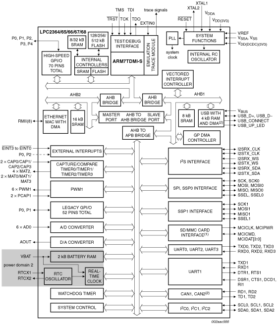
- For our application we are using:
- GPIO pins to communicate with and control devices on the same node
- CAN bus to communicate with other nodes and the Flight Computer
- USB to communicate with devices on this and other nodes as well as the Flight Computer
- I2C to communicate with devices on this node
- A/D to read devices on this node
- External 32.678 kHz crystal for RTC clock
- External 12.0 MHz crystal for internal PLL and sync to switching power supplies in the SPS and HAP
- Various Reset, test, control and debug lines.
Interface Description
    Information from the LPC2368 web site
    CAN
    USB
    I2C
    Analog
    Clocks
Pin Descriptions
    From the Web site
Pin Connections
    What pin goes where, why? x100
    What GPIO pins are in use
    What GPIO pins are available?
GLUE Devices
    Part#
    Part Description
    Purpose
    Specifications/Calculations
The following is a listing of the LPC2368 pins used in the generic node. The far right column indicates whether a pin is available for use during design of non-generic nodes.
| Sort by Signal | || | || | Sort by Pin and Purpose (Generic Node Only) | |||||
|---|---|---|---|---|---|---|---|---|
| Pin | Signal | || | || | Pin | Signal | Destination | Available | |
| 46 | PORT0.0/RD1/TXD3/SDA1 | || | || | 1 | TDO | Debug-P7 | no | |
| 47 | PORT0.1/TD1/RXD3/SCL1 | || | || | 2 | TDI | Debug-P6 | no | |
| 98 | PORT0.2/TXD0 | || | || | 3 | TMS | Debug-P8 | no | |
| 99 | PORT0.3/RXD0 | || | || | 4 | !TRST | Debug-P9 | no | |
| 81 | PORT0.4/I2SRX_CLK/RD2/CAP2.0 | || | || | 5 | TCK | Debug-P5 | no | |
| 80 | PORT0.5/I2SRX_WS/TD2/CAP2.1 | || | || | 6 | PORT0.26/AD0.3/AOUT/RXD3 | No-connect | yes | |
| 79 | PORT0.6/I2SRX_SDA/SSEL1/MAT2.0 | || | || | 7 | PORT0.25/AD0.2/I2SRX_SDA/TXD3 | No-connect | yes | |
| 78 | PORT0.7/I2STX_CLK/SCK1/MAT2.1 | || | || | 8 | PORT0.24/AD0.1/I2SRX_WS/CAP3.1 | No-connect | yes | |
| 77 | PORT0.8/I2STX_WS/MISO1/MAT2.2 | || | || | 9 | PORT0.23/AD0.0/I2SRX_CLK/CAP3.0 | No-connect | yes | |
| 76 | PORT0.9/I2STX_SDA/MOSI1/MAT2.3 | || | || | 10 | VDDA | A_3P3 | no | |
| 48 | PORT0.10/TXD2/SDA2/MAT3.0 | || | || | 11 | VSSA | A_GND | no | |
| 49 | PORT0.11/RXD2/SCL2/MAT3.1 | || | || | 12 | VREF | CPU_VREF | no | |
| 62 | PORT0.15/TXD1/SCK0/SCK | || | || | 13 | VDD(DCDC)(3V3) | 3.3VHAPOUT | no | |
| 63 | PORT0.16/RXD1/SSEL0/SSEL | || | || | 14 | !RSTOUT | Debug-P3 | no | |
| 61 | PORT0.17/CTS1/MISO0/MISO | || | || | 15 | VSS | GND | no | |
| 60 | PORT0.18/DCD1/MOSI0/MOSI | || | || | 16 | RTCX1 | RTC_XTAL-A | no | |
| 59 | PORT0.19/DSR1/MCICLK/SDA1 | || | || | 17 | !RESET | Debug-P2 | no | |
| 58 | PORT0.20/DTR1/MCICMD/SCL1 | || | || | 18 | RTCX2 | RTC_XTAL-B | no | |
| 57 | PORT0.21/RI1/MCIPWR/RD1 | || | || | 19 | VBAT | CPU_VBAT | no | |
| 56 | PORT0.22/RTS1/MCIDAT0/TD1 | || | || | 20 | PORT1.31/SCK1/AD0.5 | BATCHRGMONITOR | no | |
| 9 | PORT0.23/AD0.0/I2SRX_CLK/CAP3.0 | || | || | 21 | PORT1.30/VBUS/AD0.4 | No-connect | yes | |
| 8 | PORT0.24/AD0.1/I2SRX_WS/CAP3.1 | || | || | 22 | XTAL1 | CPU_XTAL1 | no | |
| 7 | PORT0.25/AD0.2/I2SRX_SDA/TXD3 | || | || | 23 | XTAL2 | CPU_XTAL2 | no | |
| 6 | PORT0.26/AD0.3/AOUT/RXD3 | || | || | 24 | PORT0.28/SCL0 | No-connect | yes | |
| 25 | PORT0.27/SDA0 | || | || | 25 | PORT0.27/SDA0 | No-connect | yes | |
| 24 | PORT0.28/SCL0 | || | || | 26 | PORT3.26/MAT0.1/RXD3 | No-connect | yes | |
| 29 | PORT0.29/USB_D+ | || | || | 27 | PORT3.25/MAT0.0/PWM1.2 | No-connect | yes | |
| 30 | PORT0.30/USB_D- | || | || | 28 | VDD(3V3) | 3.3VHAPOUT | no | |
| 95 | PORT1.0/ENET_TXD0 | || | || | 29 | PORT0.29/USB_D+ | USB_D+ | no | |
| 94 | PORT1.1/ENET_TXD1 | || | || | 30 | PORT0.30/USB_D- | USB_D- | no | |
| 93 | PORT1.4/ENETTXEN | || | || | 31 | VSS@1 | GND | no | |
| 92 | PORT1.8/ENET_CRS | || | || | 32 | PORT1.18/USBUPLED/PWM1.1/CAP1.0 | GPIOUSBHighSpeed | no | |
| 91 | PORT1.9/ENET_RXD0 | || | || | 33 | PORT1.19/CAP1.1 | No-connect | yes | |
| 90 | PORT1.10/ENET_RXD1 | || | || | 34 | PORT1.20/PWM1.2/SCK0 | No-connect | yes | |
| 89 | PORT1.14/ENETRXER | || | || | 35 | PORT1.21/PWM1.3/SSEL0 | No-connect | yes | |
| 88 | PORT1.15/ENETREFCLK | || | || | 36 | PORT1.22/MAT1.0 | No-connect | yes | |
| 87 | PORT1.16/ENET_MDC | || | || | 37 | PORT1.23/PWM1.4/MISO0 | No-connect | yes | |
| 86 | PORT1.17/ENET_MDIO | || | || | 38 | PORT1.24/PWM1.5/MOSI0 | No-connect | yes | |
| 32 | PORT1.18/USBUPLED/PWM1.1/CAP1.0 | || | || | 39 | PORT1.25/MAT1.1 | No-connect | yes | |
| 33 | PORT1.19/CAP1.1 | || | || | 40 | PORT1.26/PWM1.6/CAP0.0 | No-connect | yes | |
| 34 | PORT1.20/PWM1.2/SCK0 | || | || | 41 | VSS@2 | GND | no | |
| 35 | PORT1.21/PWM1.3/SSEL0 | || | || | 42 | VDD(DCDC)(3V3)@1 | 3.3VHAPOUT | no | |
| 36 | PORT1.22/MAT1.0 | || | || | 43 | PORT1.27/CAP0.1 | No-connect | yes | |
| 37 | PORT1.23/PWM1.4/MISO0 | || | || | 44 | PORT1.28/PCAP1.0/MAT0.0 | No-connect | yes | |
| 38 | PORT1.24/PWM1.5/MOSI0 | || | || | 45 | PORT1.29/PCAP1.1/MAT0.1 | No-connect | yes | |
| 39 | PORT1.25/MAT1.1 | || | || | 46 | PORT0.0/RD1/TXD3/SDA1 | CAN | no | |
| 40 | PORT1.26/PWM1.6/CAP0.0 | || | || | 47 | PORT0.1/TD1/RXD3/SCL1 | CAN | no | |
| 43 | PORT1.27/CAP0.1 | || | || | 48 | PORT0.10/TXD2/SDA2/MAT3.0 | No-connect | yes | |
| 44 | PORT1.28/PCAP1.0/MAT0.0 | || | || | 49 | PORT0.11/RXD2/SCL2/MAT3.1 | No-connect | yes | |
| 45 | PORT1.29/PCAP1.1/MAT0.1 | || | || | 50 | PORT2.13/!EINT3/MCIDAT3/I2STX_SDA | No-connect | yes | |
| 21 | PORT1.30/VBUS/AD0.4 | || | || | 51 | PORT2.12/!EINT2/MCIDAT2/I2STX_WS | No-connect | yes | |
| 20 | PORT1.31/SCK1/AD0.5 | || | || | 52 | PORT2.11/!EINT1/MCIDAT1/I2STX_CLK | No-connect | yes | |
| 75 | PORT2.0/PWM1.1/TXD1/TRACECLK | || | || | 53 | PORT2.10/!EINT0 | Debug-P10 | no | |
| 74 | PORT2.1/PWM1.2/RXD1/PIPESTAT0 | || | || | 54 | VDD(3V3)@1 | 3.3VHAPOUT | no | |
| 53 | PORT2.10/!EINT0 | || | || | 55 | VSS@3 | GND | no | |
| 52 | PORT2.11/!EINT1/MCIDAT1/I2STX_CLK | || | || | 56 | PORT0.22/RTS1/MCIDAT0/TD1 | No-connect | yes | |
| 51 | PORT2.12/!EINT2/MCIDAT2/I2STX_WS | || | || | 57 | PORT0.21/RI1/MCIPWR/RD1 | No-connect | yes | |
| 50 | PORT2.13/!EINT3/MCIDAT3/I2STX_SDA | || | || | 58 | PORT0.20/DTR1/MCICMD/SCL1 | No-connect | yes | |
| 73 | PORT2.2/PWM1.3/CTS1/PIPESTAT1 | || | || | 59 | PORT0.19/DSR1/MCICLK/SDA1 | No-connect | yes | |
| 70 | PORT2.3/PWM1.4/DCD1/PIPESTAT2 | || | || | 60 | PORT0.18/DCD1/MOSI0/MOSI | No-connect | yes | |
| 69 | PORT2.4/PWM1.5/DSR1/TRACESYNC | || | || | 61 | PORT0.17/CTS1/MISO0/MISO | No-connect | yes | |
| 68 | PORT2.5/PWM1.6/DTR1/TRACEPKT0 | || | || | 62 | PORT0.15/TXD1/SCK0/SCK | No-connect | yes | |
| 67 | PORT2.6/PCAP1.0/RI1/TRACEPKT1 | || | || | 63 | PORT0.16/RXD1/SSEL0/SSEL | No-connect | yes | |
| 66 | PORT2.7/RD2/RTS1/TRACEPKT2 | || | || | 64 | PORT2.9/USB_CONNECT/RXD2/EXTIN0 | No-connect | yes | |
| 65 | PORT2.8/TD2/TXD2/TRACEPKT3 | || | || | 65 | PORT2.8/TD2/TXD2/TRACEPKT3 | No-connect | yes | |
| 64 | PORT2.9/USB_CONNECT/RXD2/EXTIN0 | || | || | 66 | PORT2.7/RD2/RTS1/TRACEPKT2 | No-connect | yes | |
| 27 | PORT3.25/MAT0.0/PWM1.2 | || | || | 67 | PORT2.6/PCAP1.0/RI1/TRACEPKT1 | No-connect | yes | |
| 26 | PORT3.26/MAT0.1/RXD3 | || | || | 68 | PORT2.5/PWM1.6/DTR1/TRACEPKT0 | No-connect | yes | |
| 82 | PORT4.28/MAT2.0/TXD3 | || | || | 69 | PORT2.4/PWM1.5/DSR1/TRACESYNC | No-connect | yes | |
| 85 | PORT4.29/MAT2.1/RXD3 | || | || | 70 | PORT2.3/PWM1.4/DCD1/PIPESTAT2 | No-connect | yes | |
| 17 | !RESET | || | || | 71 | VDD(3V3)@2 | 3.3VHAPOUT | no | |
| 14 | !RSTOUT | || | || | 72 | VSS@4 | GND | no | |
| 100 | RTCK | || | || | 73 | PORT2.2/PWM1.3/CTS1/PIPESTAT1 | No-connect | yes | |
| 16 | RTCX1 | || | || | 74 | PORT2.1/PWM1.2/RXD1/PIPESTAT0 | No-connect | yes | |
| 18 | RTCX2 | || | || | 75 | PORT2.0/PWM1.1/TXD1/TRACECLK | No-connect | yes | |
| 5 | TCK | || | || | 76 | PORT0.9/I2STX_SDA/MOSI1/MAT2.3 | No-connect | yes | |
| 2 | TDI | || | || | 77 | PORT0.8/I2STX_WS/MISO1/MAT2.2 | No-connect | yes | |
| 1 | TDO | || | || | 78 | PORT0.7/I2STX_CLK/SCK1/MAT2.1 | No-connect | yes | |
| 3 | TMS | || | || | 79 | PORT0.6/I2SRX_SDA/SSEL1/MAT2.0 | No-connect | yes | |
| 4 | !TRST | || | || | 80 | PORT0.5/I2SRX_WS/TD2/CAP2.1 | No-connect | yes | |
| 19 | VBAT | || | || | 81 | PORT0.4/I2SRX_CLK/RD2/CAP2.0 | CAN_Autobaud | no | |
| 28 | VDD(3V3) | || | || | 82 | PORT4.28/MAT2.0/TXD3 | No-connect | yes | |
| 54 | VDD(3V3)@1 | || | || | 83 | VSS@6 | GND | no | |
| 71 | VDD(3V3)@2 | || | || | 84 | VDD(DCDC)(3V3)@2 | 3.3VHAPOUT | no | |
| 96 | VDD(3V3)@3 | || | || | 85 | PORT4.29/MAT2.1/RXD3 | No-connect | yes | |
| 13 | VDD(DCDC)(3V3) | || | || | 86 | PORT1.17/ENET_MDIO | StatusLED2 | no | |
| 42 | VDD(DCDC)(3V3)@1 | || | || | 87 | PORT1.16/ENET_MDC | StatusLED1 | no | |
| 84 | VDD(DCDC)(3V3)@2 | || | || | 88 | PORT1.15/ENETREFCLK | No-connect | yes | |
| 10 | VDDA | || | || | 89 | PORT1.14/ENETRXER | GPIOHAPDISABLE | no | |
| 12 | VREF | || | || | 90 | PORT1.10/ENET_RXD1 | GPIOBAT!CHRG! | no | |
| 15 | VSS | || | || | 91 | PORT1.9/ENET_RXD0 | GPIOCHRGRDIS_B | no | |
| 31 | VSS@1 | || | || | 92 | PORT1.8/ENET_CRS | GPIOCHRGRDIS_A | no | |
| 41 | VSS@2 | || | || | 93 | PORT1.4/ENETTXEN | GPIOSPS5V_GOOD | no | |
| 55 | VSS@3 | || | || | 94 | PORT1.1/ENET_TXD1 | GPIOSPSV-IN_GOOD | no | |
| 72 | VSS@4 | || | || | 95 | PORT1.0/ENET_TXD0 | GPIOSPSDISABLE | no | |
| 97 | VSS@5 | || | || | 96 | VDD(3V3)@3 | 3.3VHAPOUT | no | |
| 83 | VSS@6 | || | || | 97 | VSS@5 | GND | no | |
| 11 | VSSA | || | || | 98 | PORT0.2/TXD0 | Debug-P11 | no | |
| 22 | XTAL1 | || | || | 99 | PORT0.3/RXD0 | Debug-P12 | no | |
| 23 | XTAL2 | || | || | 100 | RTCK | Debug-P4 | no | |
The following list contains a pin to signal reference for the LPC2368 Microcontroller.
| Sort by Signal | Sort by Pin | |||
|---|---|---|---|---|
| Pin | Signal | Pin | Signal | |
| 46 | PORT0.0/RD1/TXD3/SDA1 | 1 | TDO | |
| 47 | PORT0.1/TD1/RXD3/SCL1 | 2 | TDI | |
| 98 | PORT0.2/TXD0 | 3 | TMS | |
| 99 | PORT0.3/RXD0 | 4 | !TRST | |
| 81 | PORT0.4/I2SRX_CLK/RD2/CAP2.0 | 5 | TCK | |
| 80 | PORT0.5/I2SRX_WS/TD2/CAP2.1 | 6 | PORT0.26/AD0.3/AOUT/RXD3 | |
| 79 | PORT0.6/I2SRX_SDA/SSEL1/MAT2.0 | 7 | PORT0.25/AD0.2/I2SRX_SDA/TXD3 | |
| 78 | PORT0.7/I2STX_CLK/SCK1/MAT2.1 | 8 | PORT0.24/AD0.1/I2SRX_WS/CAP3.1 | |
| 77 | PORT0.8/I2STX_WS/MISO1/MAT2.2 | 9 | PORT0.23/AD0.0/I2SRX_CLK/CAP3.0 | |
| 76 | PORT0.9/I2STX_SDA/MOSI1/MAT2.3 | 10 | VDDA | |
| 48 | PORT0.10/TXD2/SDA2/MAT3.0 | 11 | VSSA | |
| 49 | PORT0.11/RXD2/SCL2/MAT3.1 | 12 | VREF | |
| 62 | PORT0.15/TXD1/SCK0/SCK | 13 | VDD(DCDC)(3V3) | |
| 63 | PORT0.16/RXD1/SSEL0/SSEL | 14 | !RSTOUT | |
| 61 | PORT0.17/CTS1/MISO0/MISO | 15 | VSS | |
| 60 | PORT0.18/DCD1/MOSI0/MOSI | 16 | RTCX1 | |
| 59 | PORT0.19/DSR1/MCICLK/SDA1 | 17 | !RESET | |
| 58 | PORT0.20/DTR1/MCICMD/SCL1 | 18 | RTCX2 | |
| 57 | PORT0.21/RI1/MCIPWR/RD1 | 19 | VBAT | |
| 56 | PORT0.22/RTS1/MCIDAT0/TD1 | 20 | PORT1.31/SCK1/AD0.5 | |
| 9 | PORT0.23/AD0.0/I2SRX_CLK/CAP3.0 | 21 | PORT1.30/VBUS/AD0.4 | |
| 8 | PORT0.24/AD0.1/I2SRX_WS/CAP3.1 | 22 | XTAL1 | |
| 7 | PORT0.25/AD0.2/I2SRX_SDA/TXD3 | 23 | XTAL2 | |
| 6 | PORT0.26/AD0.3/AOUT/RXD3 | 24 | PORT0.28/SCL0 | |
| 25 | PORT0.27/SDA0 | 25 | PORT0.27/SDA0 | |
| 24 | PORT0.28/SCL0 | 26 | PORT3.26/MAT0.1/RXD3 | |
| 29 | PORT0.29/USB_D+ | 27 | PORT3.25/MAT0.0/PWM1.2 | |
| 30 | PORT0.30/USB_D- | 28 | VDD(3V3) | |
| 95 | PORT1.0/ENET_TXD0 | 29 | PORT0.29/USB_D+ | |
| 94 | PORT1.1/ENET_TXD1 | 30 | PORT0.30/USB_D- | |
| 93 | PORT1.4/ENETTXEN | 31 | VSS@1 | |
| 92 | PORT1.8/ENET_CRS | 32 | PORT1.18/USBUPLED/PWM1.1/CAP1.0 | |
| 91 | PORT1.9/ENET_RXD0 | 33 | PORT1.19/CAP1.1 | |
| 90 | PORT1.10/ENET_RXD1 | 34 | PORT1.20/PWM1.2/SCK0 | |
| 89 | PORT1.14/ENETRXER | 35 | PORT1.21/PWM1.3/SSEL0 | |
| 88 | PORT1.15/ENETREFCLK | 36 | PORT1.22/MAT1.0 | |
| 87 | PORT1.16/ENET_MDC | 37 | PORT1.23/PWM1.4/MISO0 | |
| 86 | PORT1.17/ENET_MDIO | 38 | PORT1.24/PWM1.5/MOSI0 | |
| 32 | PORT1.18/USBUPLED/PWM1.1/CAP1.0 | 39 | PORT1.25/MAT1.1 | |
| 33 | PORT1.19/CAP1.1 | 40 | PORT1.26/PWM1.6/CAP0.0 | |
| 34 | PORT1.20/PWM1.2/SCK0 | 41 | VSS@2 | |
| 35 | PORT1.21/PWM1.3/SSEL0 | 42 | VDD(DCDC)(3V3)@1 | |
| 36 | PORT1.22/MAT1.0 | 43 | PORT1.27/CAP0.1 | |
| 37 | PORT1.23/PWM1.4/MISO0 | 44 | PORT1.28/PCAP1.0/MAT0.0 | |
| 38 | PORT1.24/PWM1.5/MOSI0 | 45 | PORT1.29/PCAP1.1/MAT0.1 | |
| 39 | PORT1.25/MAT1.1 | 46 | PORT0.0/RD1/TXD3/SDA1 | |
| 40 | PORT1.26/PWM1.6/CAP0.0 | 47 | PORT0.1/TD1/RXD3/SCL1 | |
| 43 | PORT1.27/CAP0.1 | 48 | PORT0.10/TXD2/SDA2/MAT3.0 | |
| 44 | PORT1.28/PCAP1.0/MAT0.0 | 49 | PORT0.11/RXD2/SCL2/MAT3.1 | |
| 45 | PORT1.29/PCAP1.1/MAT0.1 | 50 | PORT2.13/!EINT3/MCIDAT3/I2STX_SDA | |
| 21 | PORT1.30/VBUS/AD0.4 | 51 | PORT2.12/!EINT2/MCIDAT2/I2STX_WS | |
| 20 | PORT1.31/SCK1/AD0.5 | 52 | PORT2.11/!EINT1/MCIDAT1/I2STX_CLK | |
| 75 | PORT2.0/PWM1.1/TXD1/TRACECLK | 53 | PORT2.10/!EINT0 | |
| 74 | PORT2.1/PWM1.2/RXD1/PIPESTAT0 | 54 | VDD(3V3)@1 | |
| 53 | PORT2.10/!EINT0 | 55 | VSS@3 | |
| 52 | PORT2.11/!EINT1/MCIDAT1/I2STX_CLK | 56 | PORT0.22/RTS1/MCIDAT0/TD1 | |
| 51 | PORT2.12/!EINT2/MCIDAT2/I2STX_WS | 57 | PORT0.21/RI1/MCIPWR/RD1 | |
| 50 | PORT2.13/!EINT3/MCIDAT3/I2STX_SDA | 58 | PORT0.20/DTR1/MCICMD/SCL1 | |
| 73 | PORT2.2/PWM1.3/CTS1/PIPESTAT1 | 59 | PORT0.19/DSR1/MCICLK/SDA1 | |
| 70 | PORT2.3/PWM1.4/DCD1/PIPESTAT2 | 60 | PORT0.18/DCD1/MOSI0/MOSI | |
| 69 | PORT2.4/PWM1.5/DSR1/TRACESYNC | 61 | PORT0.17/CTS1/MISO0/MISO | |
| 68 | PORT2.5/PWM1.6/DTR1/TRACEPKT0 | 62 | PORT0.15/TXD1/SCK0/SCK | |
| 67 | PORT2.6/PCAP1.0/RI1/TRACEPKT1 | 63 | PORT0.16/RXD1/SSEL0/SSEL | |
| 66 | PORT2.7/RD2/RTS1/TRACEPKT2 | 64 | PORT2.9/USB_CONNECT/RXD2/EXTIN0 | |
| 65 | PORT2.8/TD2/TXD2/TRACEPKT3 | 65 | PORT2.8/TD2/TXD2/TRACEPKT3 | |
| 64 | PORT2.9/USB_CONNECT/RXD2/EXTIN0 | 66 | PORT2.7/RD2/RTS1/TRACEPKT2 | |
| 27 | PORT3.25/MAT0.0/PWM1.2 | 67 | PORT2.6/PCAP1.0/RI1/TRACEPKT1 | |
| 26 | PORT3.26/MAT0.1/RXD3 | 68 | PORT2.5/PWM1.6/DTR1/TRACEPKT0 | |
| 82 | PORT4.28/MAT2.0/TXD3 | 69 | PORT2.4/PWM1.5/DSR1/TRACESYNC | |
| 85 | PORT4.29/MAT2.1/RXD3 | 70 | PORT2.3/PWM1.4/DCD1/PIPESTAT2 | |
| 17 | !RESET | 71 | VDD(3V3)@2 | |
| 14 | !RSTOUT | 72 | VSS@4 | |
| 100 | RTCK | 73 | PORT2.2/PWM1.3/CTS1/PIPESTAT1 | |
| 16 | RTCX1 | 74 | PORT2.1/PWM1.2/RXD1/PIPESTAT0 | |
| 18 | RTCX2 | 75 | PORT2.0/PWM1.1/TXD1/TRACECLK | |
| 5 | TCK | 76 | PORT0.9/I2STX_SDA/MOSI1/MAT2.3 | |
| 2 | TDI | 77 | PORT0.8/I2STX_WS/MISO1/MAT2.2 | |
| 1 | TDO | 78 | PORT0.7/I2STX_CLK/SCK1/MAT2.1 | |
| 3 | TMS | 79 | PORT0.6/I2SRX_SDA/SSEL1/MAT2.0 | |
| 4 | !TRST | 80 | PORT0.5/I2SRX_WS/TD2/CAP2.1 | |
| 19 | VBAT | 81 | PORT0.4/I2SRX_CLK/RD2/CAP2.0 | |
| 28 | VDD(3V3) | 82 | PORT4.28/MAT2.0/TXD3 | |
| 54 | VDD(3V3)@1 | 83 | VSS@6 | |
| 71 | VDD(3V3)@2 | 84 | VDD(DCDC)(3V3)@2 | |
| 96 | VDD(3V3)@3 | 85 | PORT4.29/MAT2.1/RXD3 | |
| 13 | VDD(DCDC)(3V3) | 86 | PORT1.17/ENET_MDIO | |
| 42 | VDD(DCDC)(3V3)@1 | 87 | PORT1.16/ENET_MDC | |
| 84 | VDD(DCDC)(3V3)@2 | 88 | PORT1.15/ENETREFCLK | |
| 10 | VDDA | 89 | PORT1.14/ENETRXER | |
| 12 | VREF | 90 | PORT1.10/ENET_RXD1 | |
| 15 | VSS | 91 | PORT1.9/ENET_RXD0 | |
| 31 | VSS@1 | 92 | PORT1.8/ENET_CRS | |
| 41 | VSS@2 | 93 | PORT1.4/ENETTXEN | |
| 55 | VSS@3 | 94 | PORT1.1/ENET_TXD1 | |
| 72 | VSS@4 | 95 | PORT1.0/ENET_TXD0 | |
| 97 | VSS@5 | 96 | VDD(3V3)@3 | |
| 83 | VSS@6 | 97 | VSS@5 | |
| 11 | VSSA | 98 | PORT0.2/TXD0 | |
| 22 | XTAL1 | 99 | PORT0.3/RXD0 | |
| 23 | XTAL2 | 100 | RTCK | |