Designin' dem PIC boards
Participants: Tim and Andrew. Waaaaah.
What we did: First pass design on the "processor section" of the CAN nodes. We're breaking the CAN boards up into four different independent schematics:
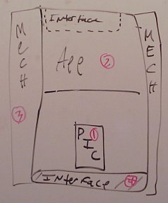
- PIC and 5V switched power supply
- Application area (node dependent)
- Standard Mechanical (for screw or card cage mounting)
- Interface connectors (CAN and power connectors)
We'll use EAGLE (http://www.cadsoft.de) to design the sections, from schematic to full on layout, and then use our vaporware Gerber editor to paste them all together to get actual "whole" boards.
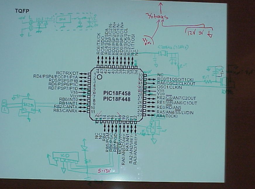
Processor Section:
Here's what we came up with for the processor section. Basically, it includes the power supply, CAN transcever, ICD interface, a voltage reference (optional to stuff), main oscillator, secondary oscillator (optional to stuff) and frankly that's it. We take more of the signals and pins and route them towards the application board (where the application circuitry can get access to the signals it needs).
Power Supply for PIC boards:
| Voltage | For what? |
|---|---|
| 12V | applications only - can take it off bus (usually for power anyway). Be carefull of shorting bus! |
| 5V | Switching regulator; main supply. |
| 3.3V | for digital chips - low current supply. Use LDO linear. |
BS'ed power consumption:
| Node | Power needed |
|---|---|
| GPS | 5V @ 200mA; power amp 5V @ 50mA = 250mA |
| IMU | 12V @ 40mA |
| PYR | ? 100mA to charge batteries? Radio = 12v @ ? Ma |
| ATV | 100mA to run BOB-II board? |
| SBS | ?? Should be off 12V supply and shore power. |
| MAG | ?? probably < 100mA |
Power Supply filter:
- Seriously considering a power supply filter: L in series with 12V & gnd, cap on other side.
- Quick calculation: 2Z(L) and Z(C) in voltage divider gives roughly 1/(w^2LC). At 500MHz, and given that we want to drop 250mV to 10mV (worst case) then with C = 10uF we get L = 10^-14 H = 0 which means that (A) it's no longer in the lumped parameter domain (think transmission line) and (B) that if we had a single turn (what the HELL is a single turn? Once through? Or once around?) a ferrite bead that'd be all we need. This is a win: very little DC drop in the turn of wire and should be able to find (or hell, make) surface mount thing.
Thus:
- Use 5V switching supply on main PIC boards
- usually don't need more than 50mA (82C250??! Check)
- Up to 250mA for GPS
- One topology with incrementally larger L and C and switch (if ext. switch)?
Things to remember:
- MOSFET switches, like on the ATV board, need to take into account some voltage difference in ground because of the ferrite beads on ground and because "we've got to think of things like Andrew routing a 32awg wire to the nose cone and back". Tim suggests a voltage divider to ground (which does gives the switch a default state, and possibly a diode.
- Think about filtering the CAN bus. We thought a bit about it, and decided that small ferrite bead that could slide over the twisted pair of the CAN bus.
Task List:
- Find a switcher chip which can be scaled from 50mA - >= 250mA w/at least 80%.
- Test 82C250 reponse to shorts (0V,5V) and check current consumption.
- Find a almost zero Henry surface mount ferrite bead loop with no DC resistance ;)